TEM Electrical Analysis
Correlate electrical activity with high resolution data
Electrical analysis in TEM plays a vital role in advancing materials science, nanotechnology, device development and failure analysis, offering insights into the behavior and properties of nanoscale materials and devices.
The Electrical Analysis system by point electronic brings all current collecting techniques, including EBIC, RCI, and EBIRCH to the STEM.
It ensures rapid, intuitive analysis and to maximize application versatility.
The system is fully integrated and software controlled and compatible with all TEMs with an external scan interface. Thanks to the hardware and software integration, it can amplify, acquire and analyse all electrical signals.
The advantages:
✅ Precise, high-quality visualization of electronic properties and defects.
✅Acquisition system is compatible with all TEMs with an external scan interface.
✅All amplification and acquisition settings are software controlled.
✅Each signal is automatically quantified and displayed in current values (µA, nA, pA).
The key features:
- Ultra-fast multi-channel imaging
- Live-color mixing
- Quantitative signal processing
- Integrated lock-in EA
- Fast amplification optimized for imaging
- Wide gain range to fit all techniques
- Miniaturized on-holder electronics
- Automated signal routing
The system consists of hardware, software and selectable options.
Explore electrical activity and high-resolution data
Use all electrical analysis techniques in TEM.
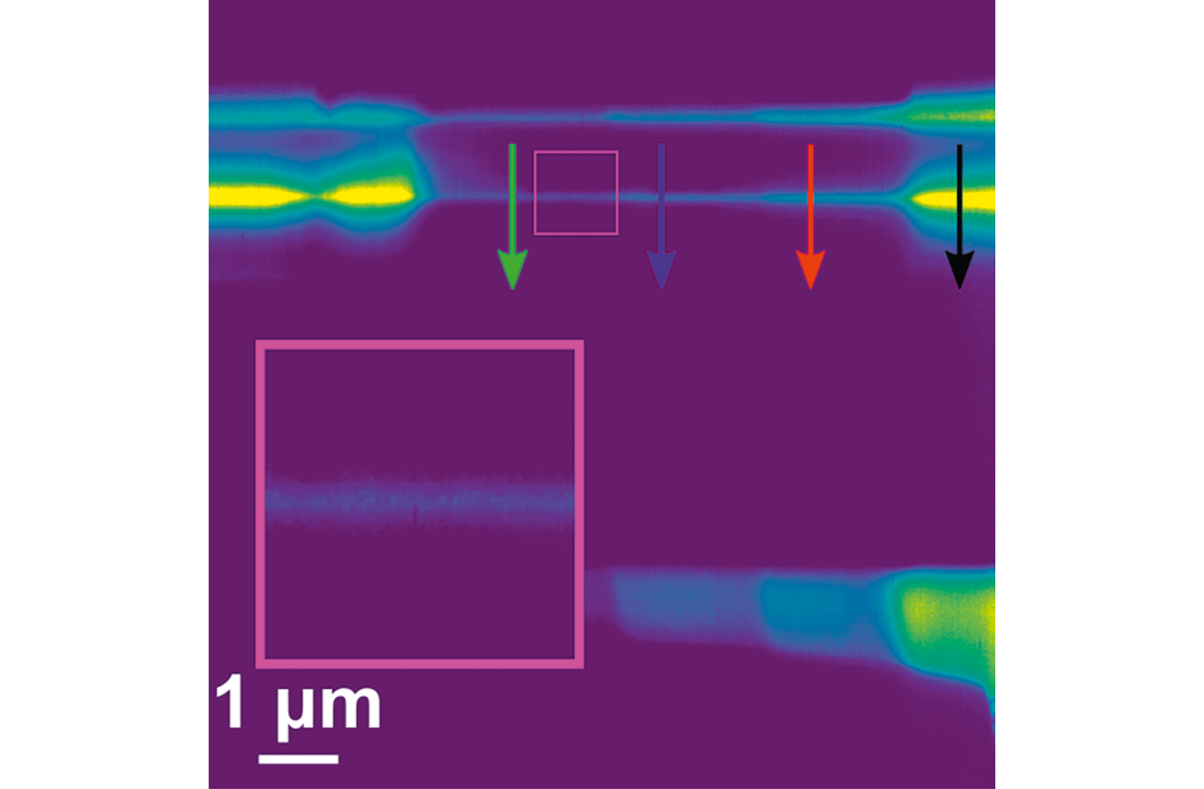
EBIC technique
Add the Electron Beam Induced Current (EBIC) technique to TEM.
Understand structure–function relationships.
Analyze device behavior.
Gain direct electrical data.
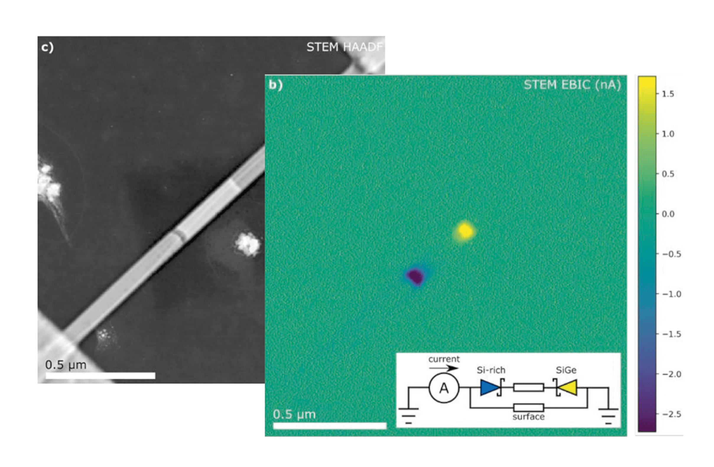
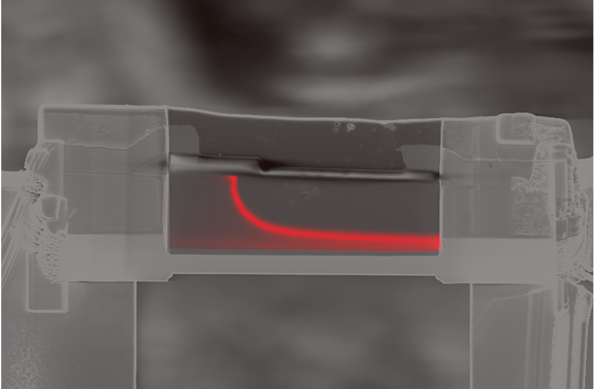
Electric fields in nanodevices
Map device junctions and contacts.
Validate doping profiles against design.
Correlate with device model and parameters.
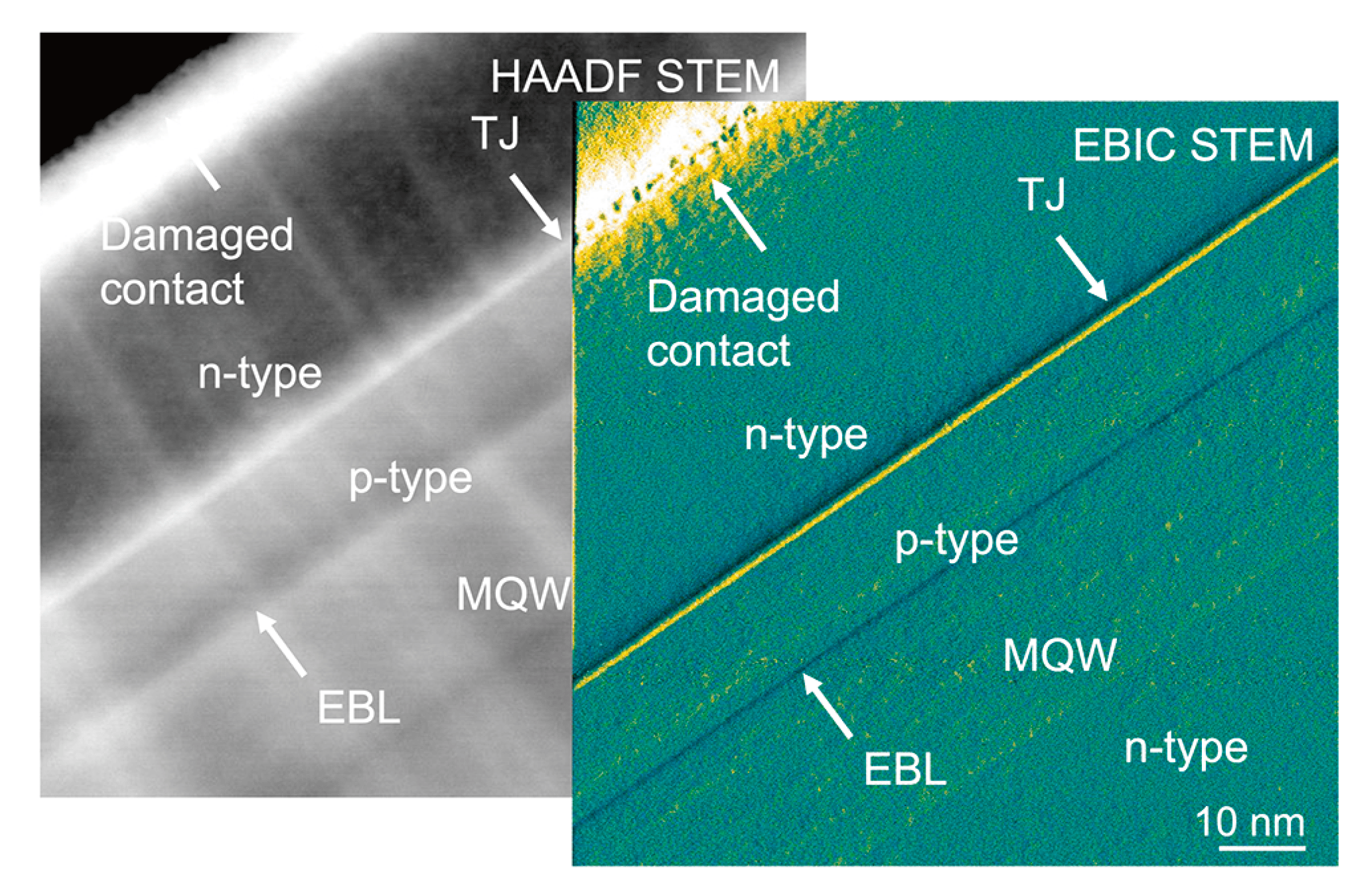
Layer analysis of complex devices
Reveal electrical activity of each layer to identify sites with increased recombination.
Distinguish electrically active defects from inactive ones.
Refine analysis with highresolution techniques.
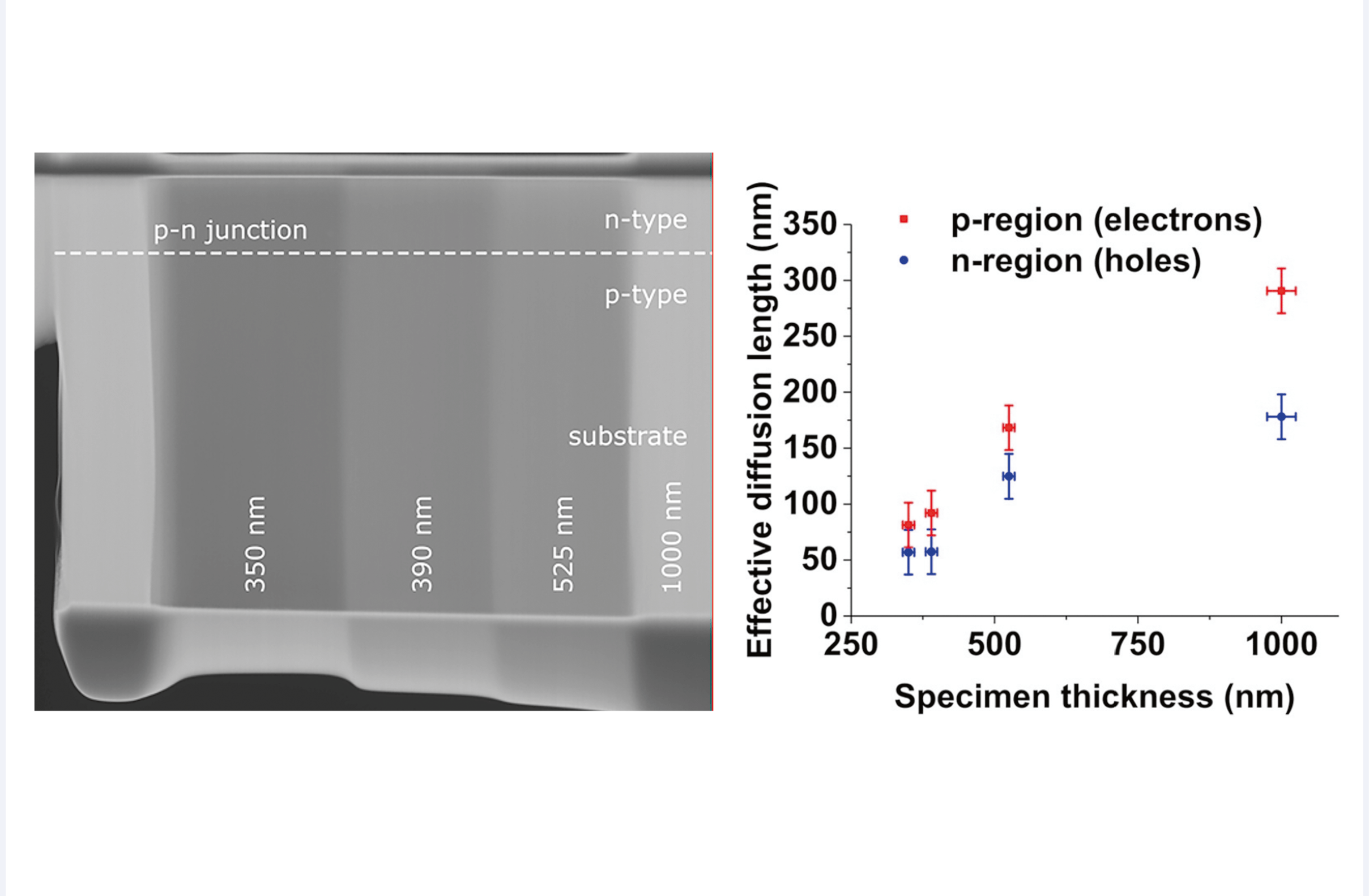
Fundamental parameters
Measure fundamental parameters including diffusion lengths, depletion width at junctions and recombination strength of dislocations.
FIB-SEM sample screening
Apply standard FIB workflows for in-situ biasing.
Use wide field-of-view of EA in SEM to select target.
Integrated and easy-to-use quantitative software
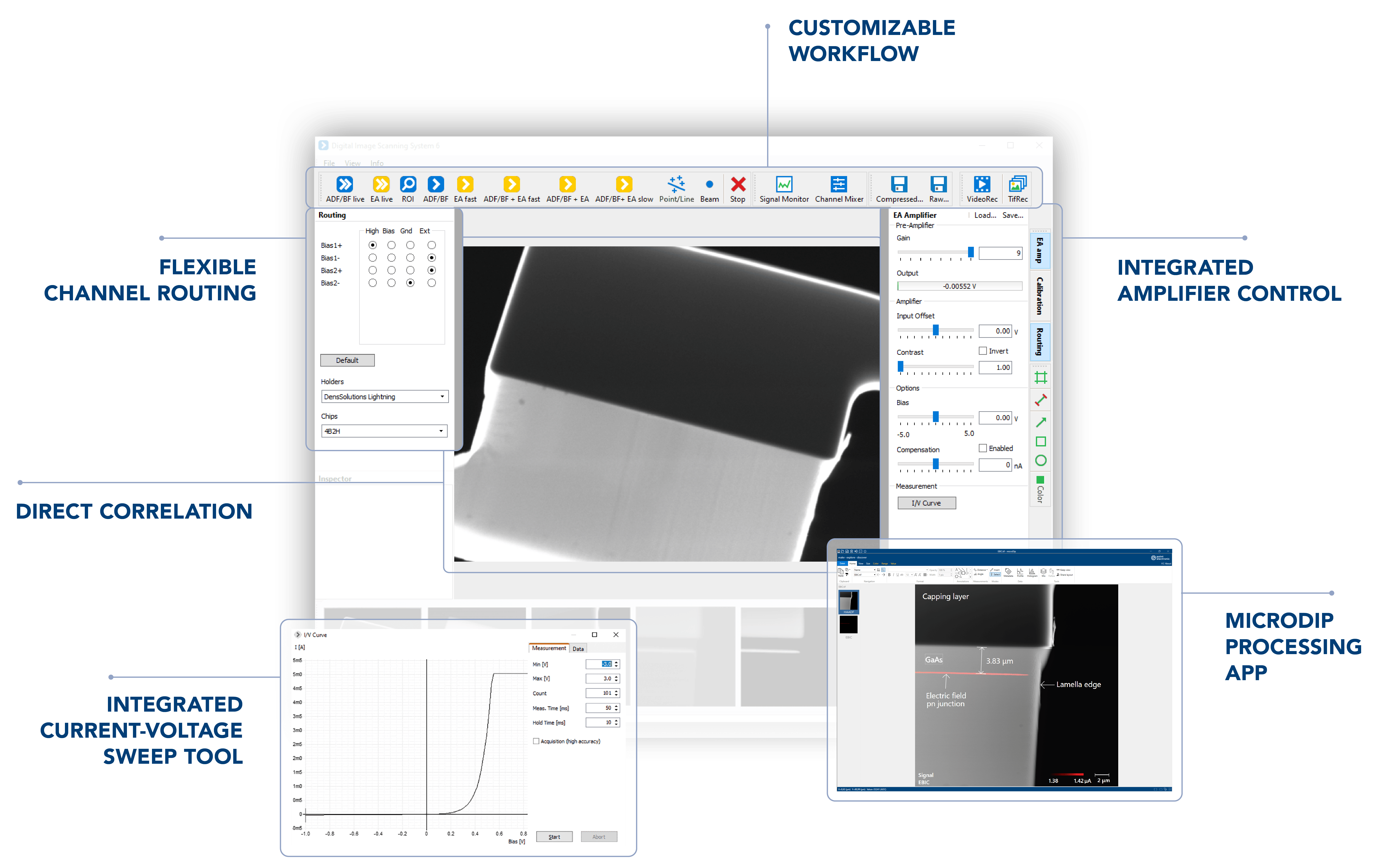
The EA Software for TEM includes EA amplifier control, EA, HAADF and BF image acquisition, a live image color-mix tool, automated quantification, a current-voltage sweep tool and standard file formats.
Customizable workflow: Creatable and configurable buttons and scan settings, including fast scan for alignment, highresolution EA profile for analysis, and simultaneous EA scan for localization.
Direct correlation: Simultaneous acquisition of Electrical Analysis with up to 20 further detector signals, live signal mixing and processing tools.
Integrated amplifier control: Software integrated, complete control of all amplifier functions, including routing, calibration, gains, offsets, bias and compensation. Auto time filter matches scan speed
Flexible channel routing: Easy distinction between SEEC, RCI and EBIC signals through software controlled channel routing.
Integrated current-voltage sweep tool: Configurable range, points, and timing to verify electrical connections and inspect for beam damage.
microDIP processing app: Full image and metadata viewer with automated quantification, gradientbased pseudo-colors, color-mix of pages, for visualization and quantitative pixel values.
Turn-key solution for in-situ EA
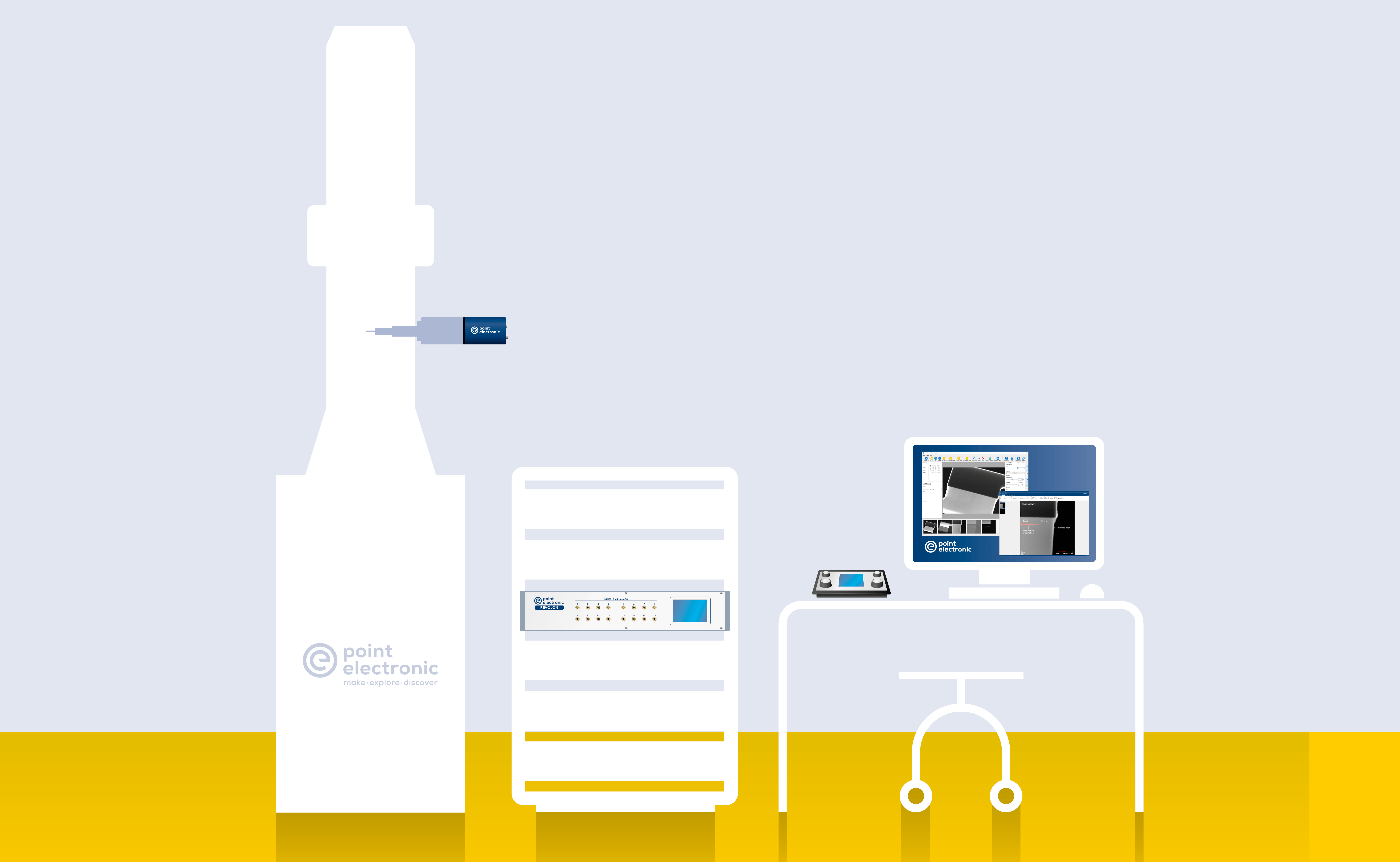
As a complete solution, all electronics are fully integrated and controlled via software.
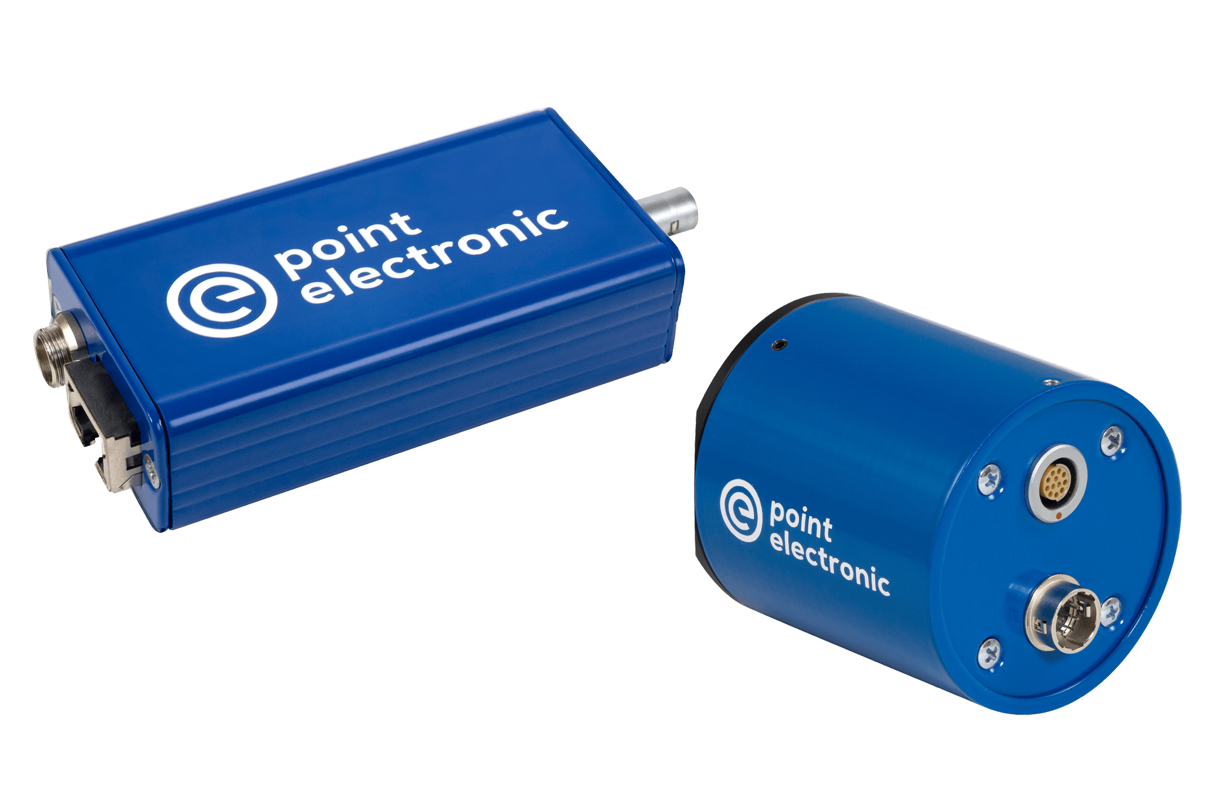
EA Amplifier options for biasing holders
First stage low-noise analog amplification with
- a wide gain range,
- built-in voltage bias and current compensation,
- automated signal routing and zero adjustment,
- and switchable low-pass filters.
Compatible with DENSSolutions and Protochips biasing holders. Other manufacturers available upon request.
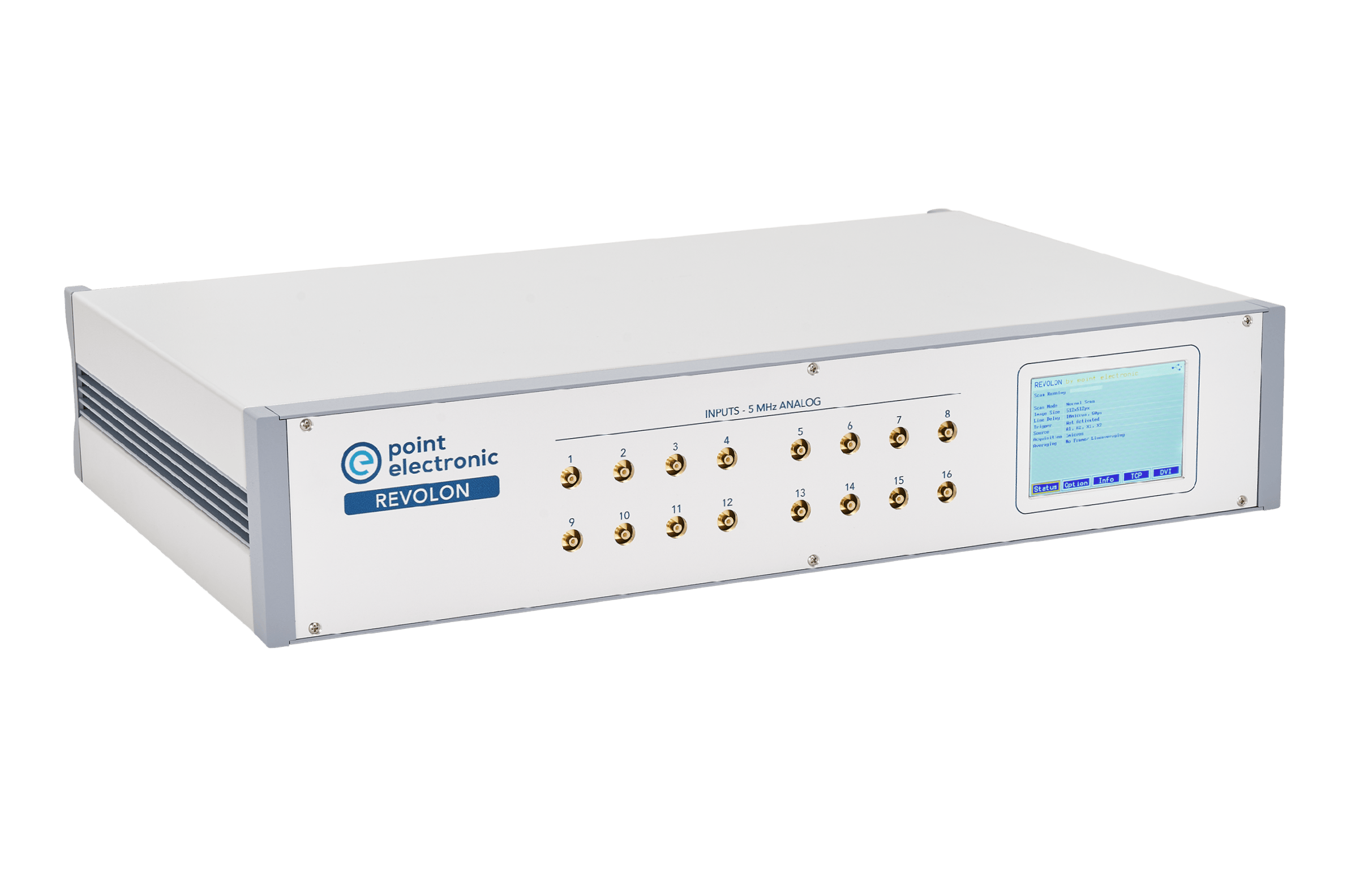
REVOLON
External TEM scan controller and imaging system for
- highest speed for in-situ STEM,
- large pixel resolution,
- second stage digital amplification for EA, and with
- simultaneous BF, HAADF and EA inputs
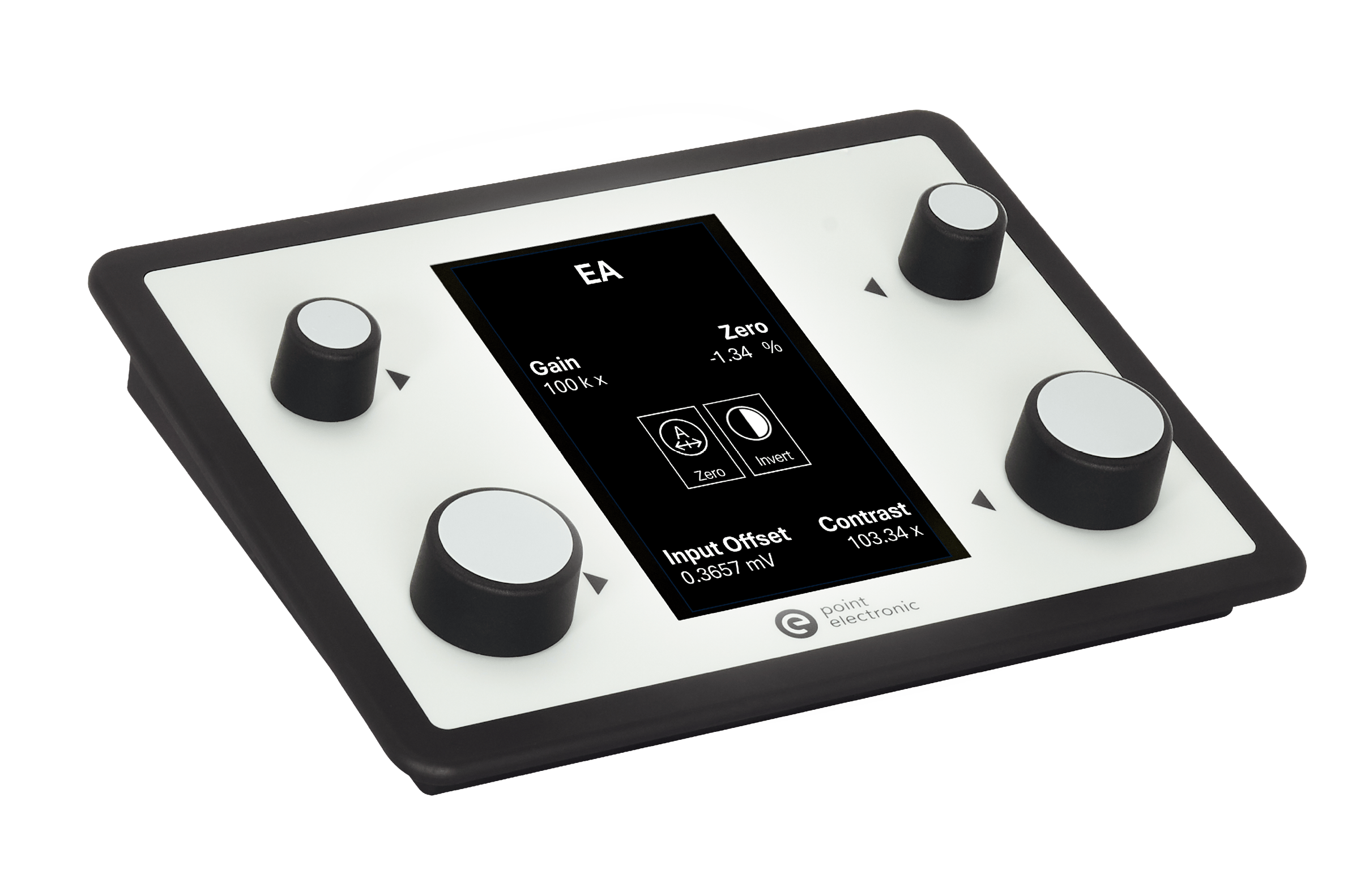
EA Control Panel
- Hardware control panel with touch display and encoders for easy, fast and precise software control.
- Fast and intuitive access to main adjustments.
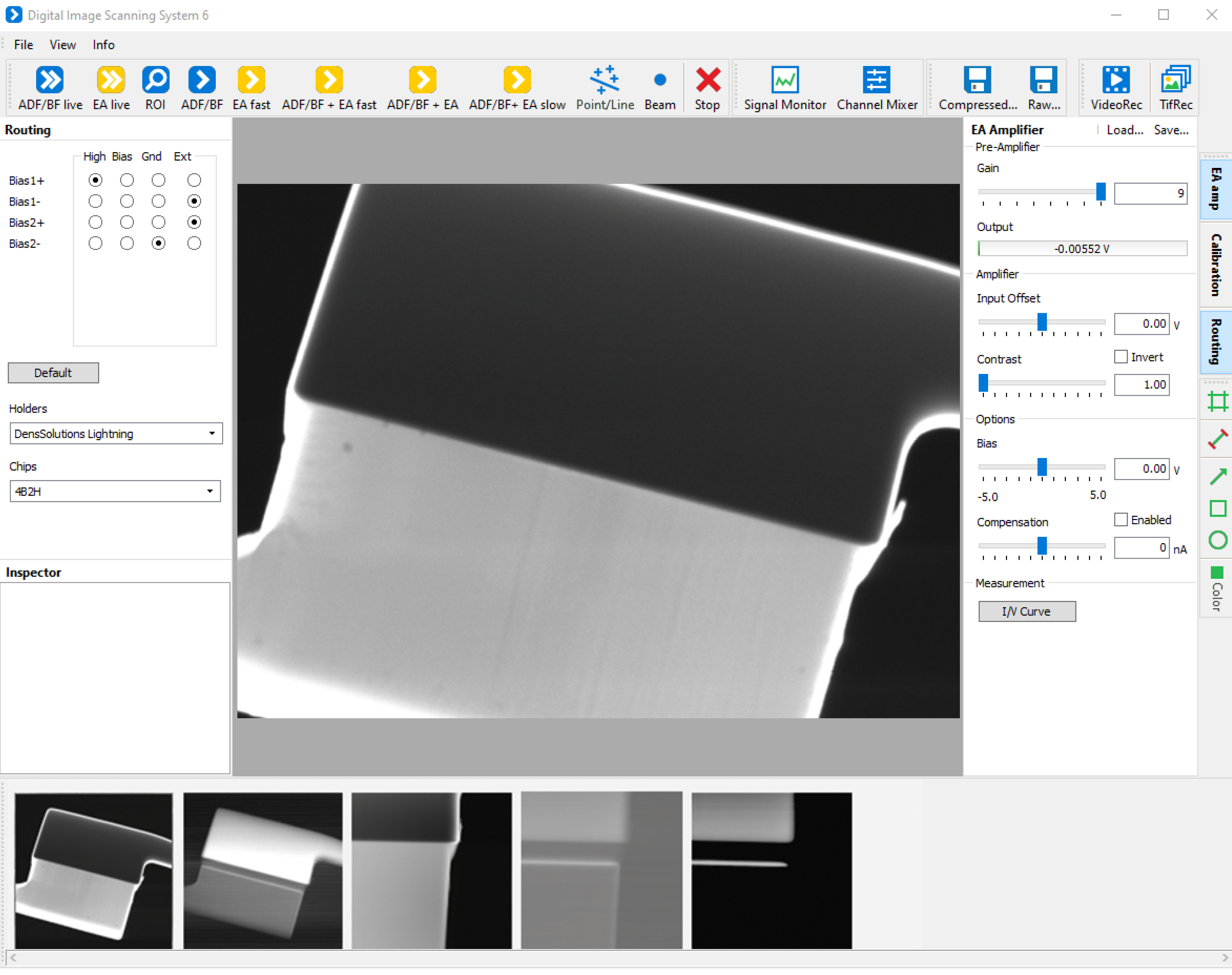
Control app
Image acquisition and amplifier control, with
- quantitative current measurement
- color mixing
- current-voltage (IV),
- line scans, inspection and
- export functions of calibrated image data
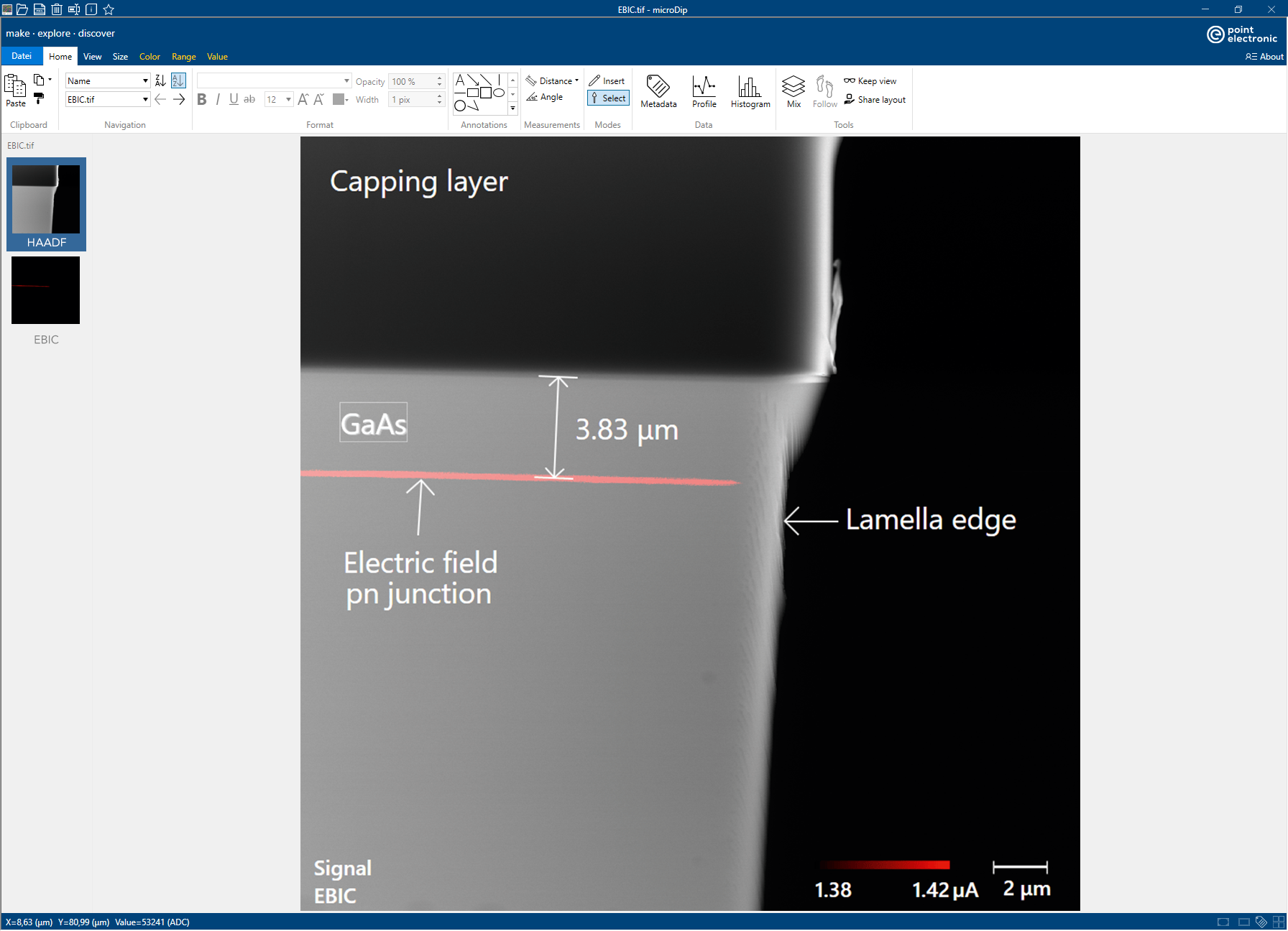
microDIP: Image post processing app
Image and metadata viewer with
- automatedpixel value quantification,
- color palette,
- signal mixing,
- line profile extraction and
- measurement of diffusion length
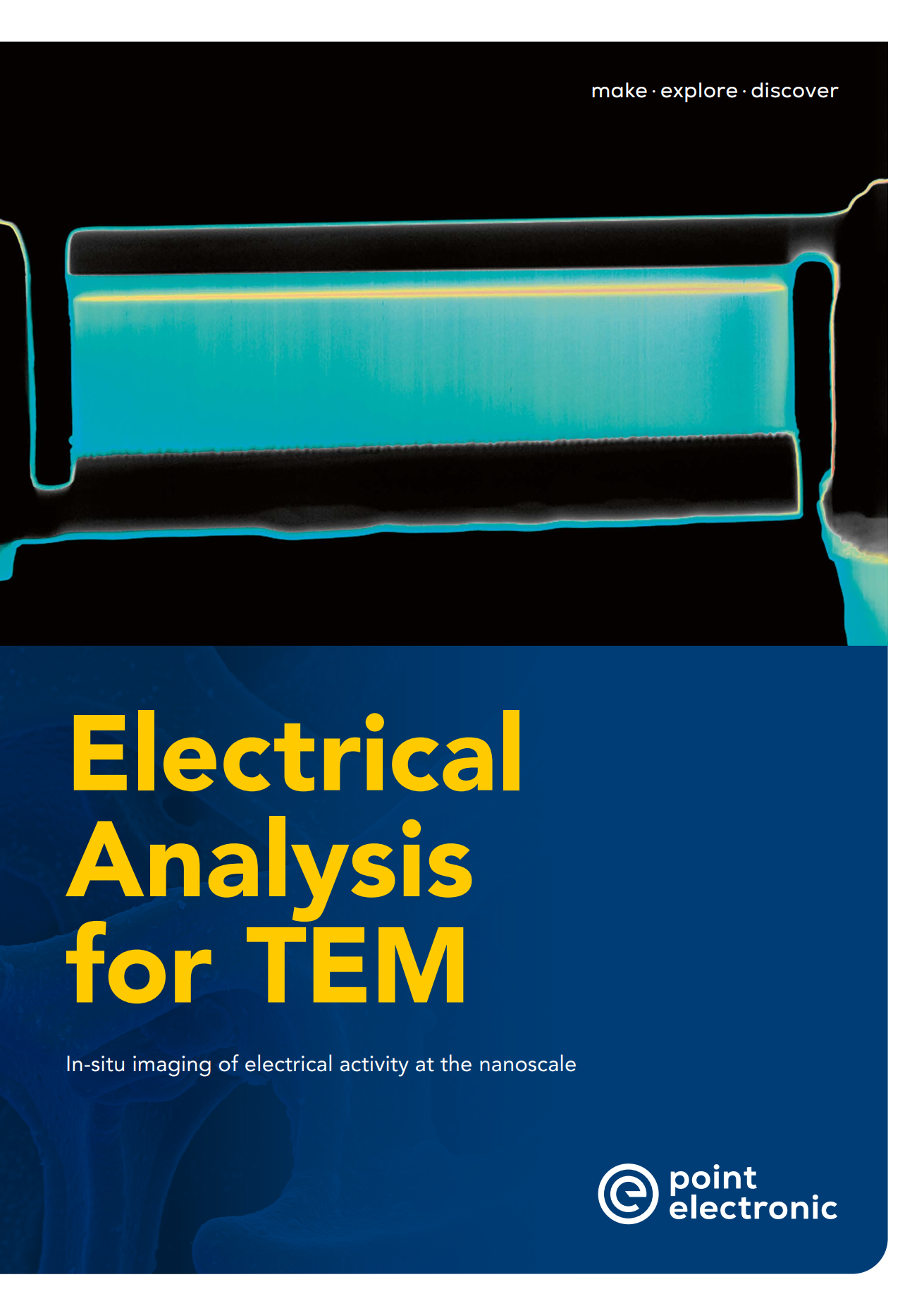
Electrical Analysis for TEM - brochure
In-situ imaging of electrical activity at the nanoscale.