TEM Electrical Analysis
Correlate electrical activity with high resolution data
Electrical analysis in TEM plays a vital role in advancing materials science, nanotechnology, device development and failure analysis, offering insights into the behavior and properties of nanoscale materials and devices.
The Electrical Analysis system by point electronic brings all current collecting techniques, including EBIC, RCI, and EBIRCH to the STEM.
It ensures rapid, intuitive analysis and to maximize application versatility.
The system is fully integrated and software controlled and compatible with all TEMs with an external scan interface. Thanks to the hardware and software integration, it can amplify, acquire and analyse all electrical signals.
The advantages:
- Precise, high-quality visualization of electronic properties and defects.
- Acquisition system is compatible with all TEMs with an external scan interface.
- All amplification and acquisition settings are software controlled.
- Each signal is automatically quantified and displayed in current values (µA, nA, pA).
The key features:
- Ultra-fast multi-channel imaging
- Live-color mixing
- Quantitative signal processing
- Integrated lock-in EA
- Fast amplification optimized for imaging
- Wide gain range to fit all techniques
- Miniaturized on-holder electronics
- Automated signal routing
The system consists of hardware, software and selectable options.
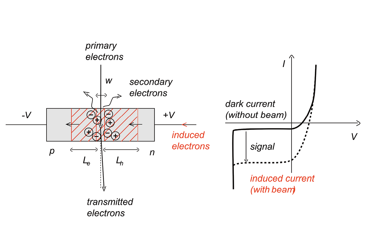
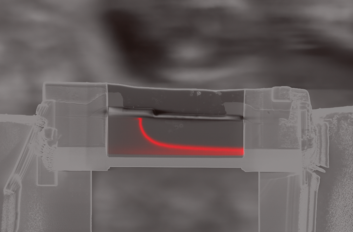
EBIC in TEM
- Inelastic loss induces electron-hole pairs in the lamella
- Internal electric fields separate electrons and holes
- Current is measured to acquire EBIC STEM images
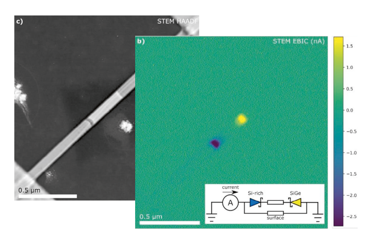
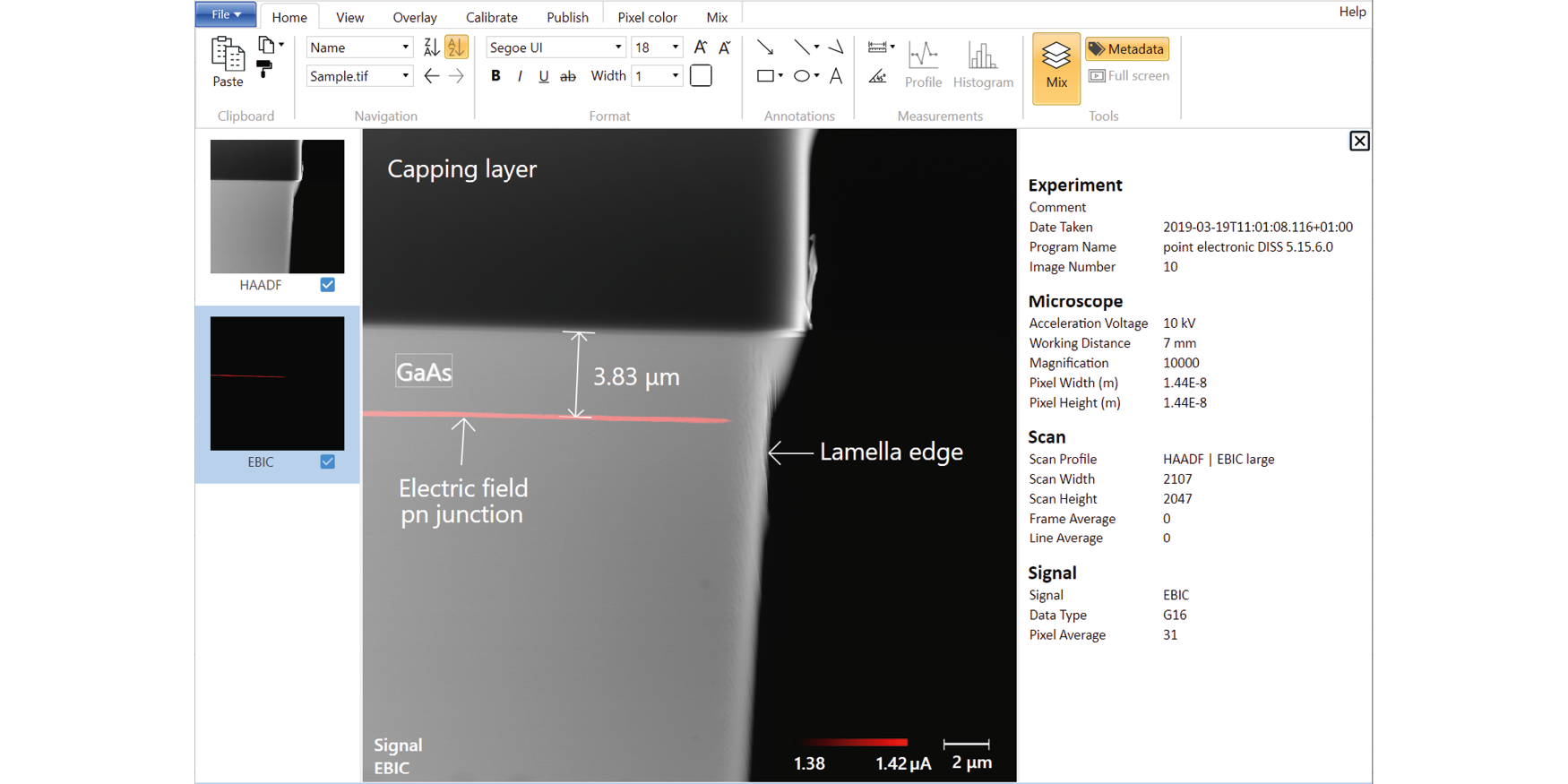
Internal electric fields
- Map junctions and contacts in devices
- Validate doping profiles against design
- Correlate with device model and parameters
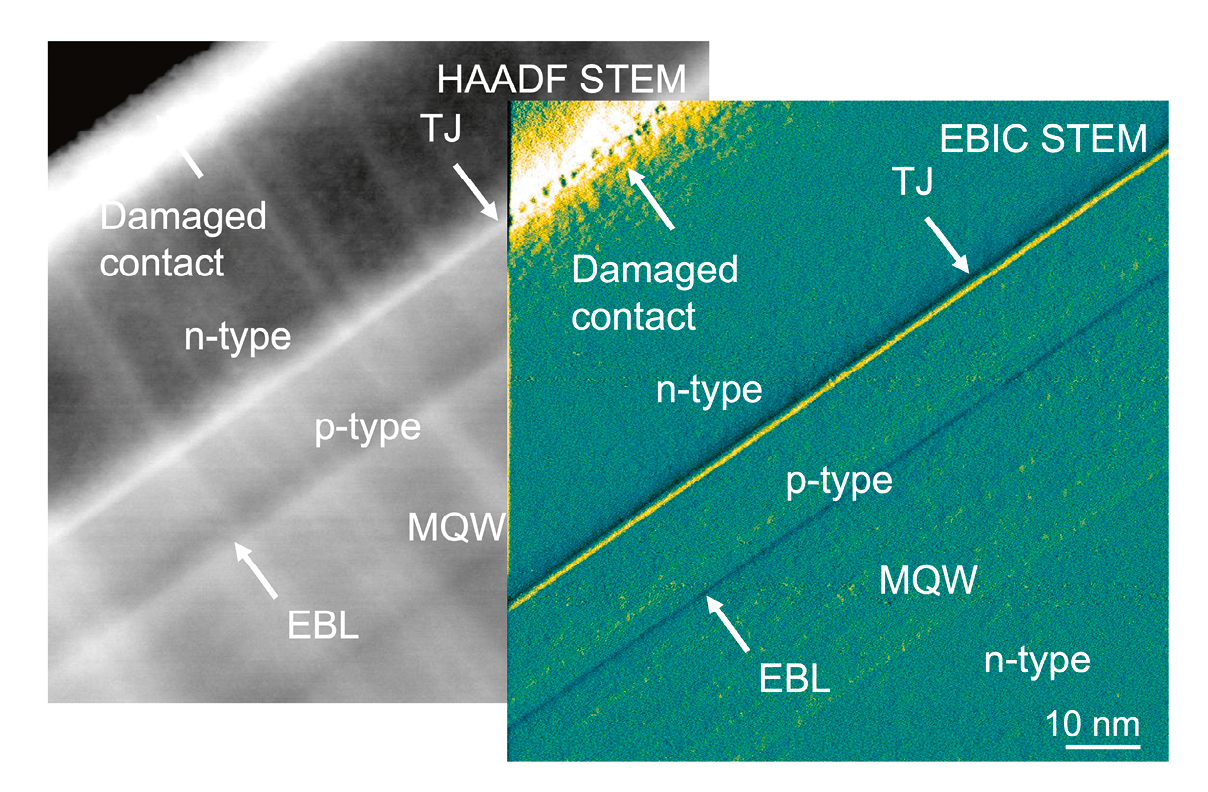
Electrical layer activity
- Localize sites with increased recombination activity
- Distinguish defects with/without electrical activity
- Continue with high-resolution techniques
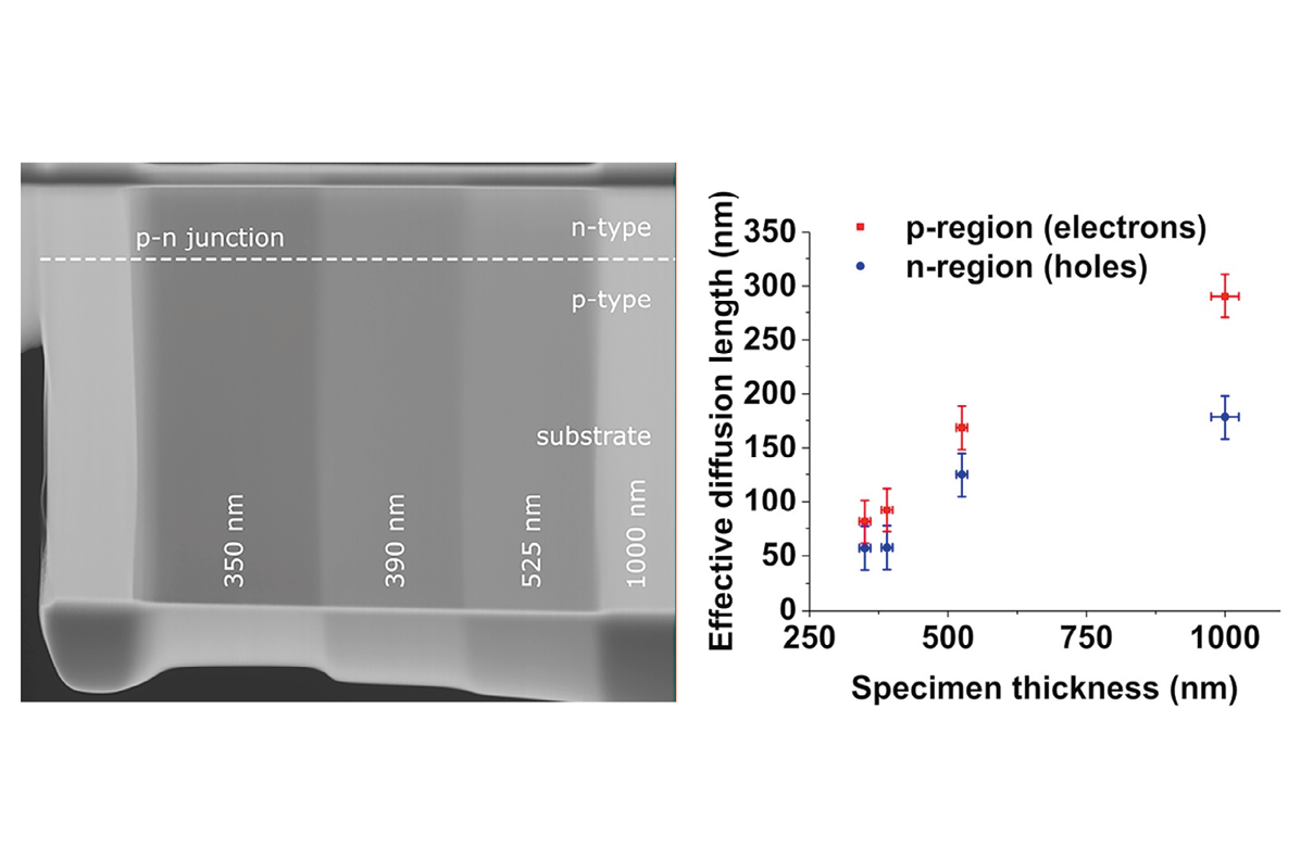
Parameter determination
- Depletion width at junctions
- Diffusion length of minority carriers
- Recombination strength of dislocations
FIB sample screening
- Apply standard FIB workflows for in-situ biasing
- Use wide field-of-view of EA in SEM to select target
- Verify lamellas in SEM for preparation damage

REVOLON TEM Scan Controller
- Integrated scan generator and image acquisition
- Large pixel resolution and high scanning speed
- Second stage digital amplification for EA
- Simultaneous BF, HAADF and EA inputs

EA electronics for in-situ biasing holders
- First stage analog amplification for minimum noise
- Wide gain range for all EA techniques and samples
- Built-in voltage bias and current compensation
- Automated signal routing to avoid electric discharge
- Switchable low passes for signal filtering
- Automated zero adjustment

EA image aquisition software
- Integrated software for image acquisition and amplifier control
- Advanced tools for colour mixing, current-voltage (IV) and line scans
- Inspection and export functions of calibrated image data
DIPS6 image processing
- Dedicated software for display of image data
- Inspection of acquisition settings in metadata
- Extraction of quantitative pixel value

Scan Control Software
- Open and independent access to scan parameters and hardware synchronisation
- Display of live images with all simultaneous signals
- Advanced scan modes, including sub-pixel and chopping
- Integrates with Python for remote network control