Electrical Failure Analysis
Electrical Failure Analysis system for SEM and STEM - from fault localization to fault characterization
Electrical failure analysis in electron microscopes is a crucial investigative technique across various industries, like semiconductor manufacturing, automotive, electronics manufacturing, medical devices or renewable energies. Analysts use it to detect microscopic defects, visualize internal structures of components, to enhance the design and manufacturing processes and in the end to improve the reliability and performance of electronic devices.
This EFA system allows fast and easy localisation with live colour mix during navigation. It offers the widest range of EFA cases with in-situ electronics for low impedance failures and the best images for reports and analysis, with dedicated image acquisition. The EFA system includes easy-to-use, fully automated calibration for current measurements.
The system consists of hardware, software and selectable options.
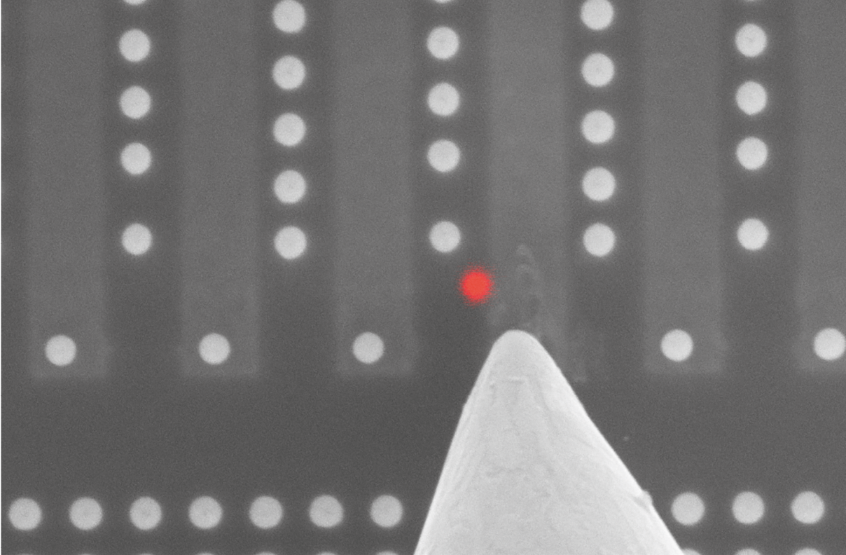
EFA techniques
- Electron Beam Induced Current (EBIC)
- Electron Beam Absorbed Current (EBAC)
- Resistive Contrast Imaging (EBAC/RCI)
- Electron Beam Induced Resistance Change (EBIRCh)
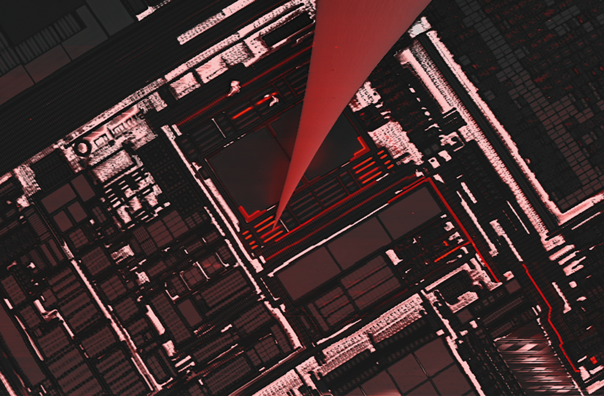
Interconnects characterisation
- Reveal electrical integrity of nets with sub-micron lateral resolution and bridge from EFA to PFA
- Diagnose fabrication and long term issues, including contamination, metal patterning defects, resistive interconnectors, or electro-migration
- Directly isolate defects to the exact layer and die location
- Improve time to product improvement actions
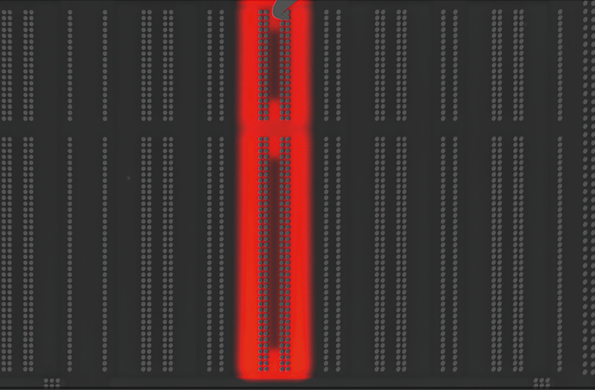
Junction and defects mapping
- Correlate structural defects with electrical activity
- Map active areas of junctions and electrical fields
- Validate doping profiles and areas
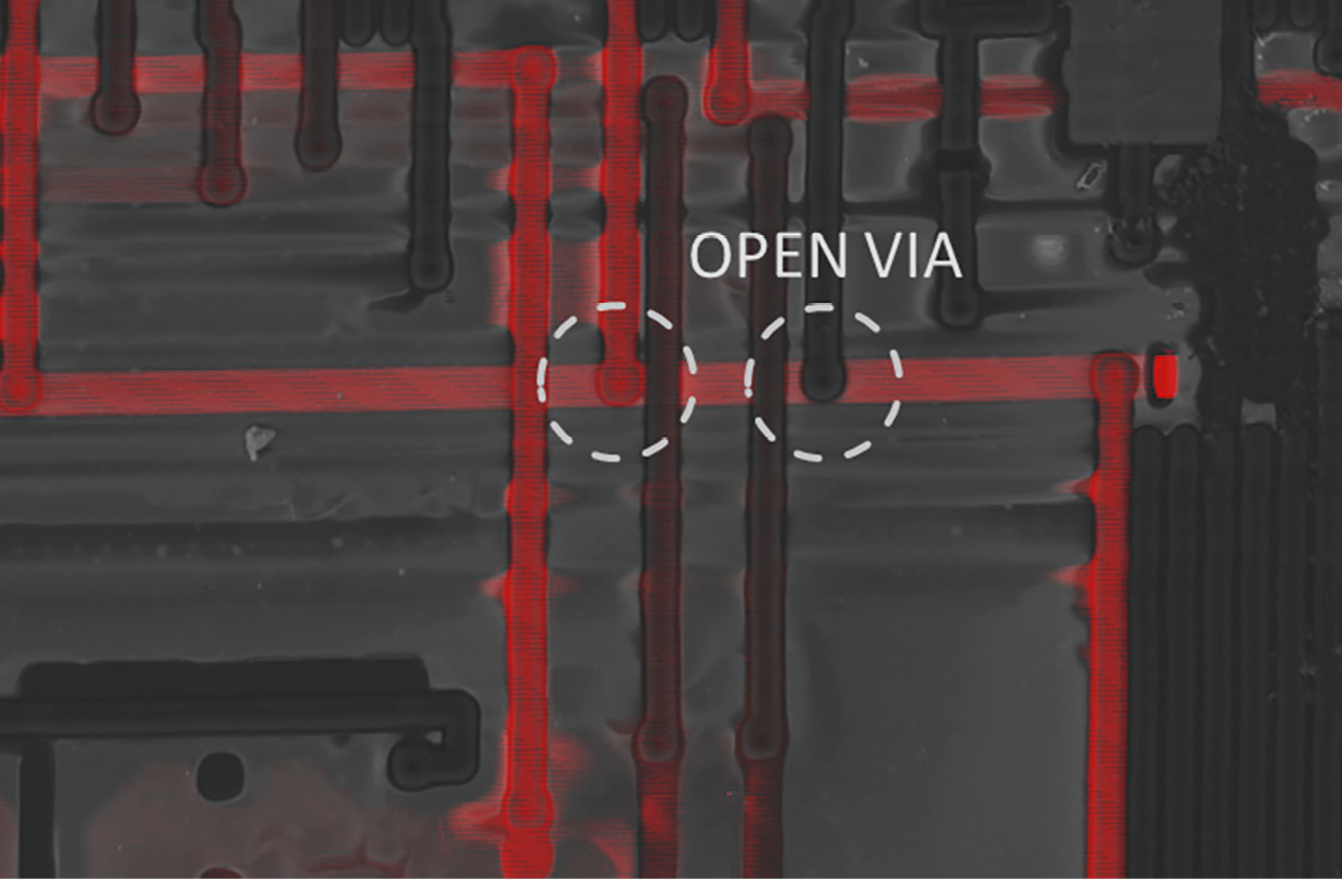
Exact localisation
- Localize metal line cuts caused by cracking, corrosion, electro-migration, or foreign particles
- Identify resistive opens caused by interface contamination at via interconnects
- Pinpoint location for direct TEM lamella FIB preparation
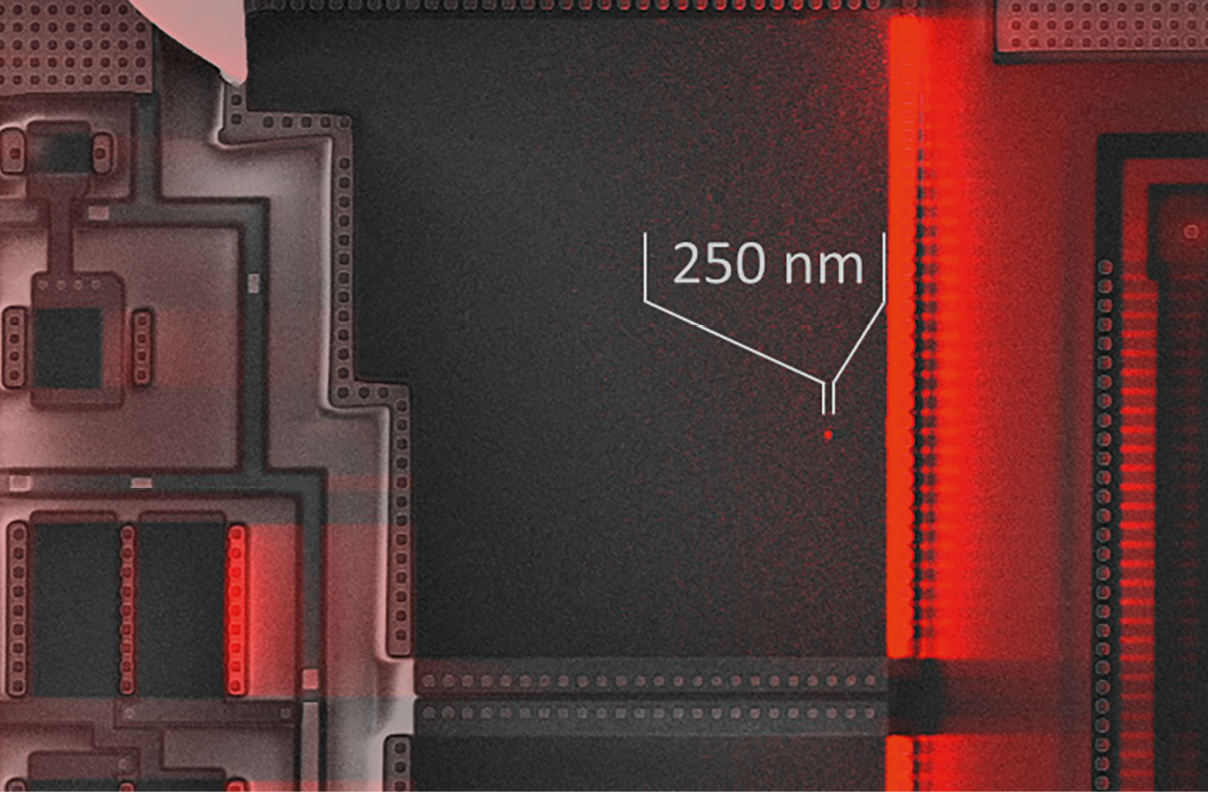
Dielectric layer defect localization
- Visualise and localise weaknesses in gate oxide (GOX) and capacitor oxide (COX) before breakdown
- Pinpoint oxide shorts caused by ESD or EOS with sub-micron resolution
- Preserve the original defect signature with power dissipation in the lower nW range during localization

Built-in biasing and live colour
- Image junctions and fields in delayered devices
- Map electrical activity of solar cells under bias
- Compare imaged behaviour with device modelling
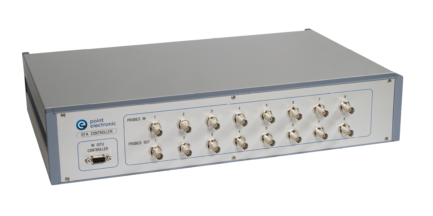
EFA Controller
- Automated routing for up to 8 probes
- In-situ electronics for low impedance failure cases
- Two stage amplification for maximum range & highest speed
- Built-in sources for voltage bias and current compensation
- New optional integrated needle cleaning PSUs
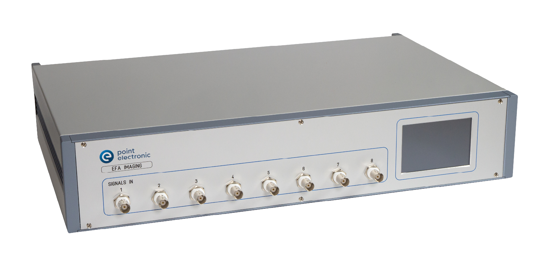
EA DISS6 Imaging
- Integrated scan generator and image acquisition
- Very large resolution and high speed
- High bit depth EFA analog-to-digital conversion
- Simultaneous SE and EFA inputs
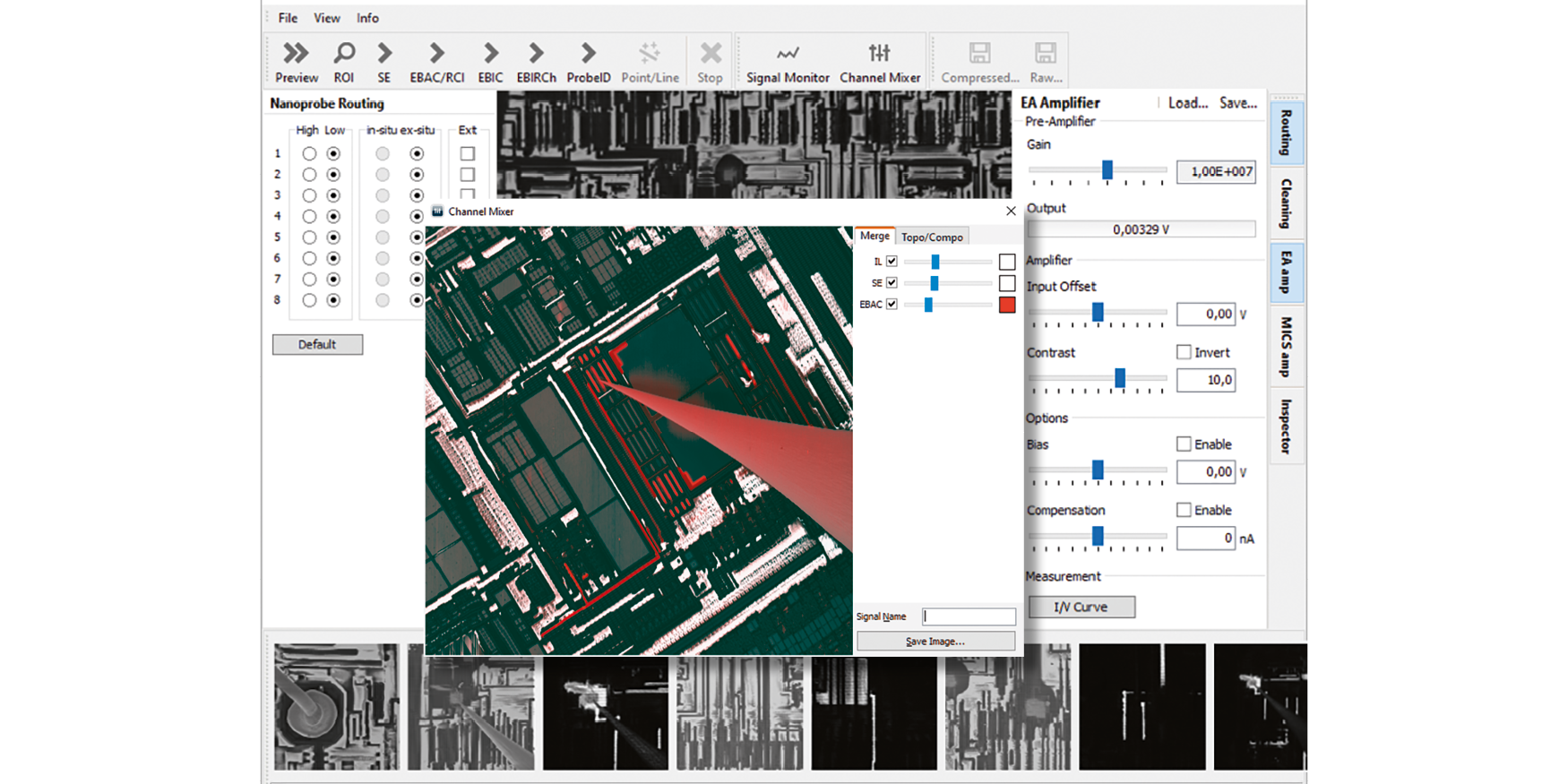
DISS6 image acquisition
- Routing and amplification control
- Live colour mix for localisation
- Current-Voltage sweep tool
- Needle cleaning tool
- Automatic quantification to fA ... µA units
- Standard file formats
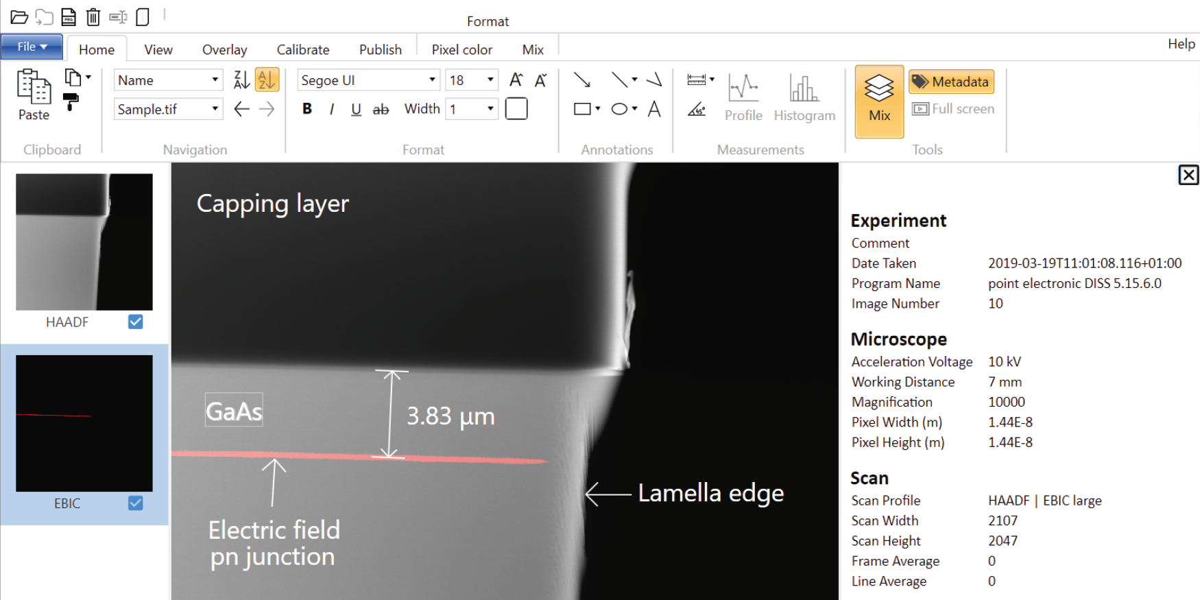
DIPS6 image processing
- Colour mix of pages for localisation
- Full image and metadata viewer
- Automatic quantification to µA...fA
- Gradient-based pseudocolours
- Export of quantitative pixel values
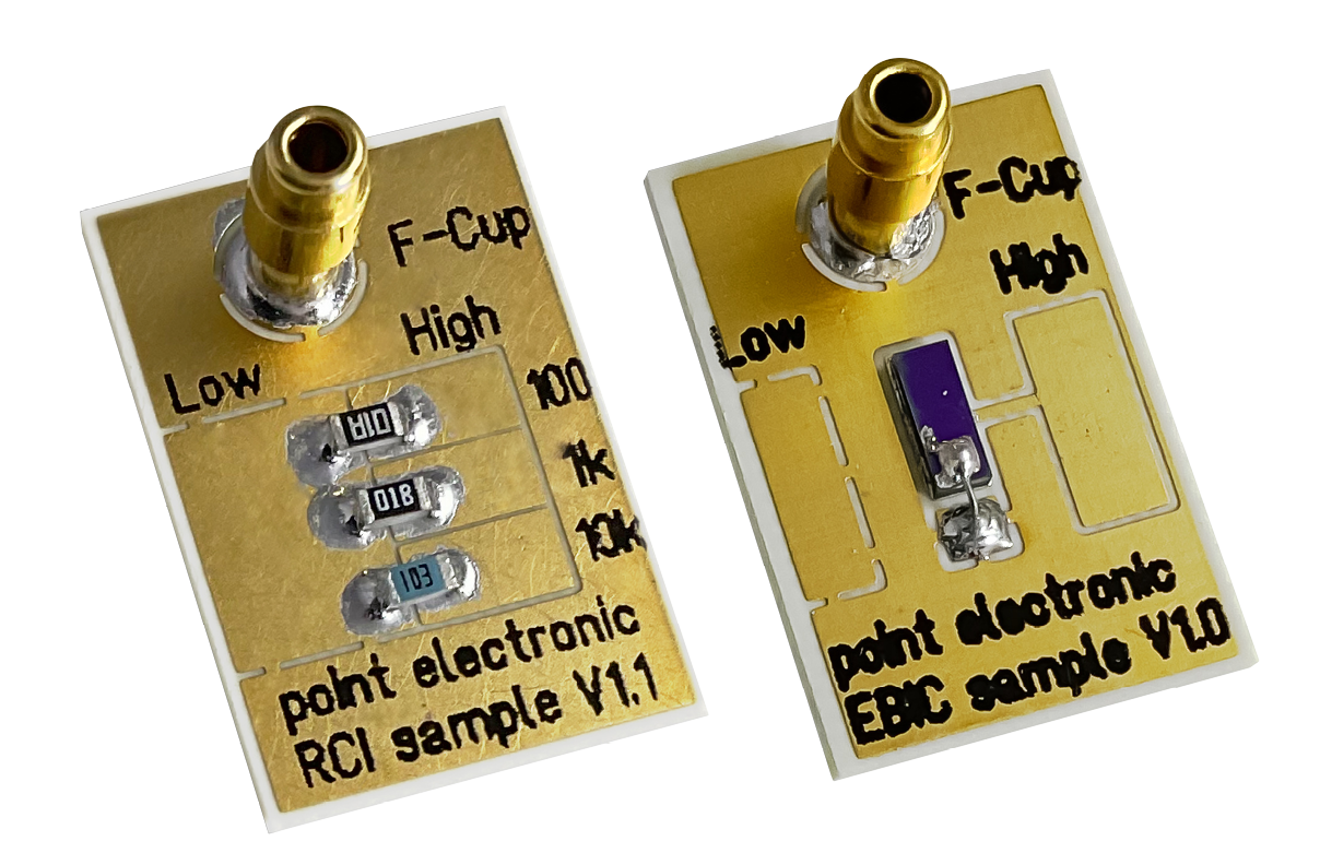
EA / EFA reference samples
- diode and resistors for reference and training
- surface mounted onto ceramic board for easy handling
- integrated Faraday cup for beam current measurements