EFA Controller
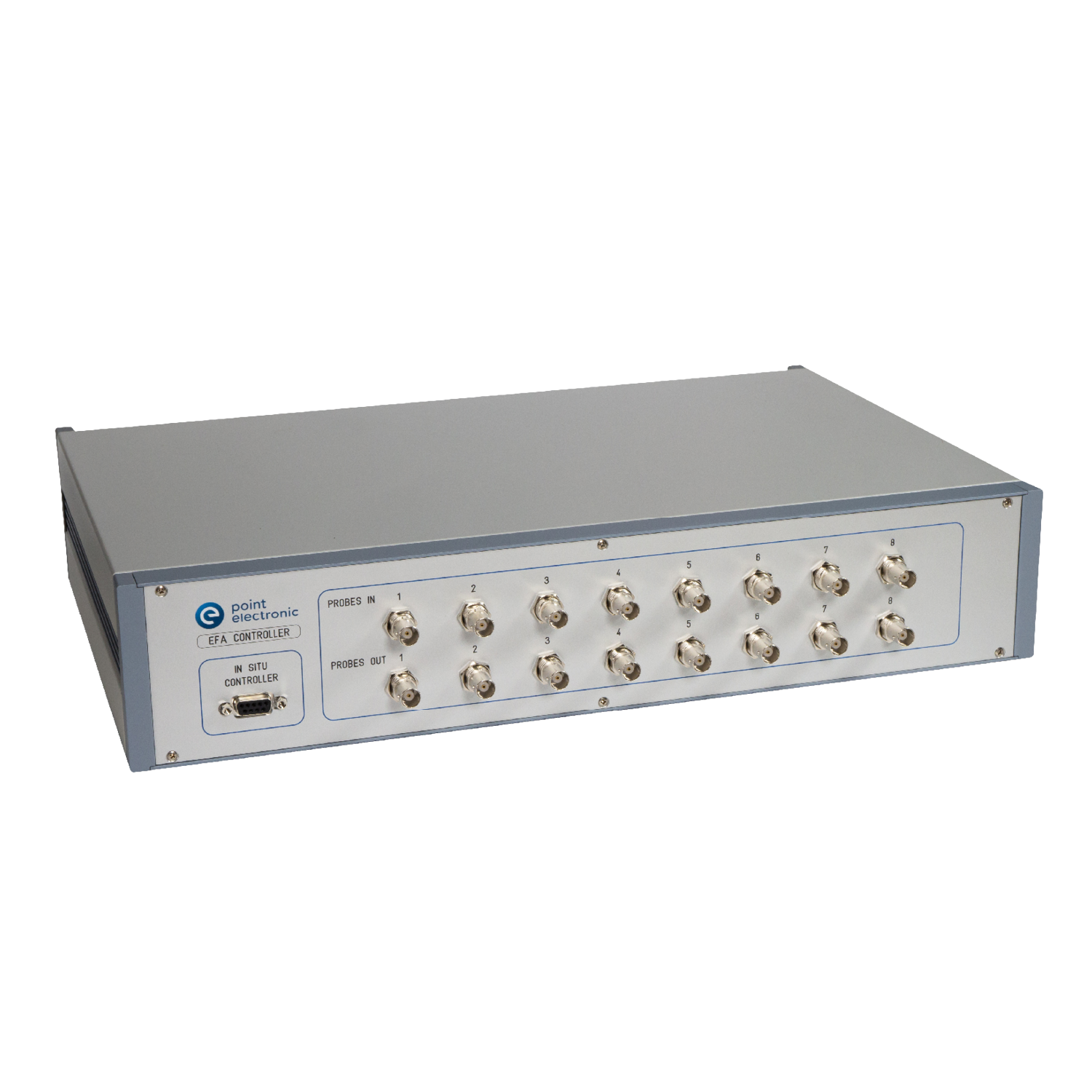
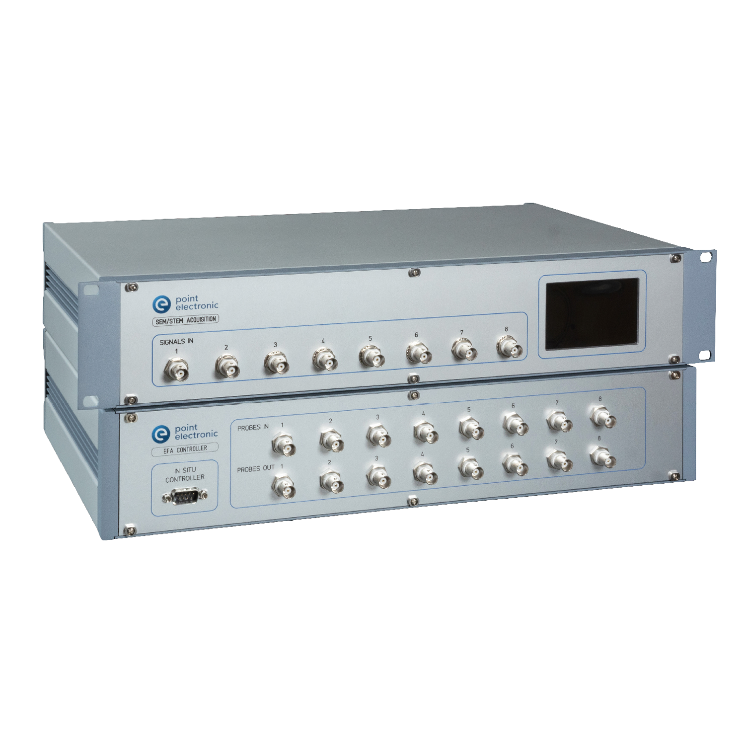
The most advanced electronics for Electrical Failure Analysis (EFA) in SEM, including routing, amplification, biasing and compensation. Controller is designed to be used with nanoprobing systems, and may be optionally equipped with in-situ electronics, power supply for probe cleaning and automatic current-voltage sweeps.
Standard features
- Automatic routing, to internal amplification, biasing or cleaning, or to external characterisation
- High-speed and low-noise transimpedance preamplifier with adjustable gain
- Lowpass filter to match amplification with imaging speed
- Second-stage amplifier for fine image adjustments
- Voltage source for device biasing
- Current source to compensate for forward or reverse signals
- Auto-zero function for calibration
Optional features
- in-situ electronics for low impedance failure cases
- current-limited voltage supply for probe cleaning
- automatic current - voltage sweeps for device characterisation
The controller is designed for a wide range of Electrical Analysis (EA) techniques

Electron Beam Induced Current (EBIC)
- map internal electric fields in semiconductors and ceramics
- characterise electrical activity of defects
- localise material and/or processing defects

Resistance Contrast Imaging (EBAC/RCI)
- localise open and shorts in inteconnects
- identify weaknesses in oxide layers
- map resistance with high spatial resolution

Electron Beam Induced Current Change (EBIRCh)
- localise defects in transistors with high-spatial resolution
- pin-point leackages/weknesses in oxides
- similar with Optical Beam Induced Resistance change (OBIRCh)
Control
- USB2 hardware interface
- device driver for Microsoft Windows
- independent control library
- integrated DISS control panel
Inputs
- 8x PROBES IN input for nanoprobing
- GND connection to microscope ground (case)
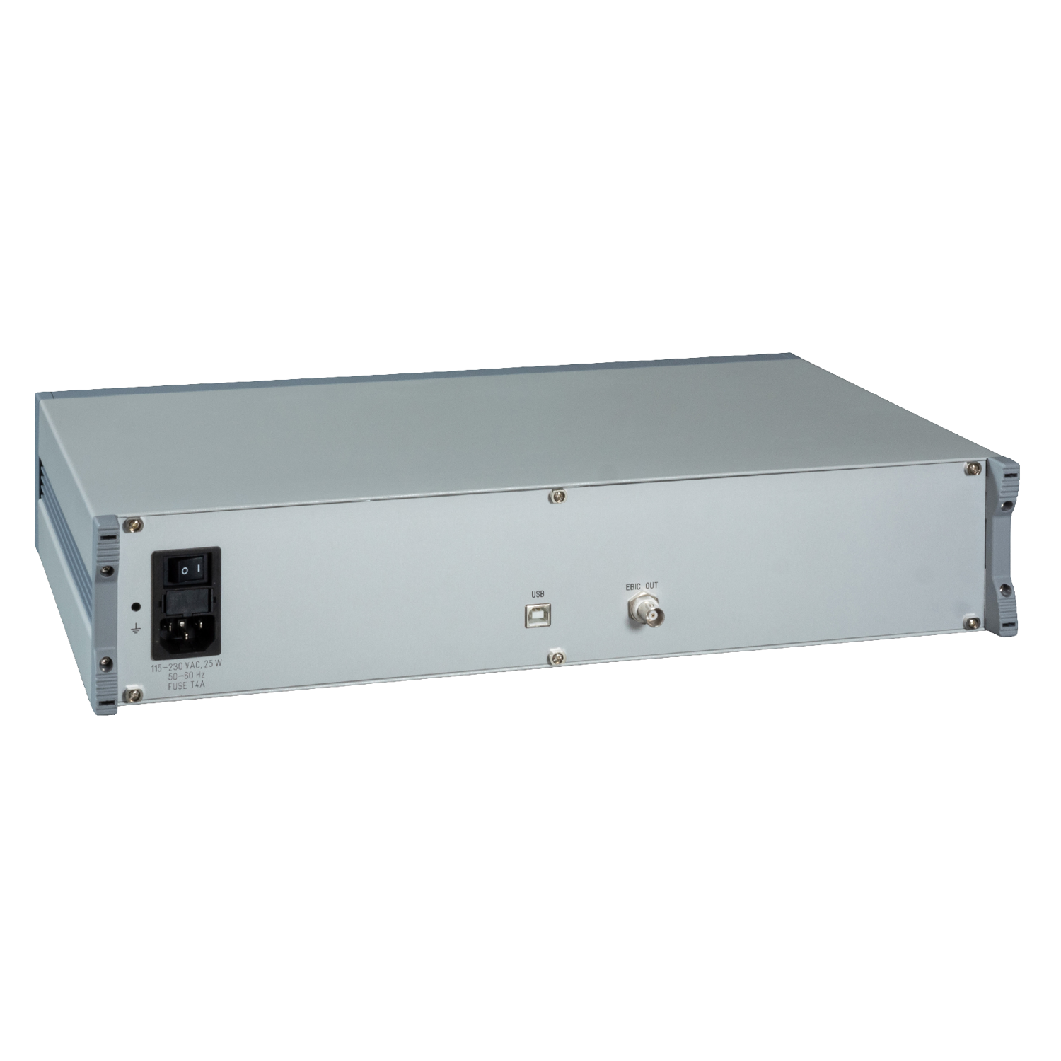
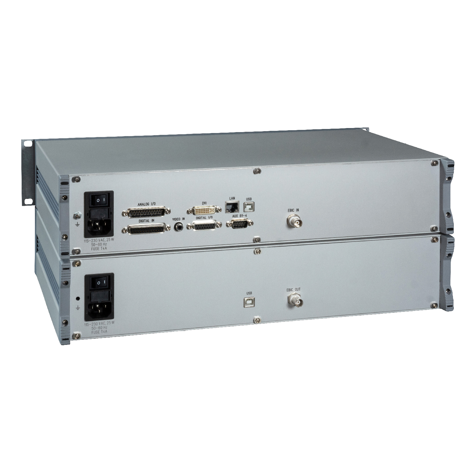
- mains input power (back panel)
Outputs
- 8x PROBES OUT for external device characterisation
- Power and control for in-situ electronics
- Amplified output for imaging (back panel)
Routing
- Automatic switching from 8x inputs to amplifier high/low
- Selection of ground, biasing and compensation on amplifier low
- Free switching to external analyser or SMUs
- Automatic routing to internal probe cleaning PSUs (optional)
Ex-situ preamplifier
- 20,000 Ohm minimum sample resistance
- 103 ... 1010 V/A configurable gain
- 8 µs minimum pixed dwell time, depending on sample impedance
- 12-bit ADC for live signal inspection
Second-stage amplifier
- -1 ... 1 µA, 16-bit input offset (brightness)
- 0.1 ... 100x, 16-bit gain (contrast)
- 0.5 MHz at 109 V/A bandwidth
- 8-levels low-pass filter
- manual signal inversion
Integrated sources
- -10 ... 10 V, 16-bit voltage bias
- -10 ... 10 µA, 16-bit current compensation
- 100 pA internal source for calibration
In-situ electronics (optional)
- 8x integrated transimpedance amplifiers and routing
- 1,000 Ohm minimum recommended sample resistance
- 107 V/A fixed transimpedanced gain
- 16 µs minimum pixed dwell time, depending on sample impedance


