Who are the partners of In-Situ Microscopy Alliance?
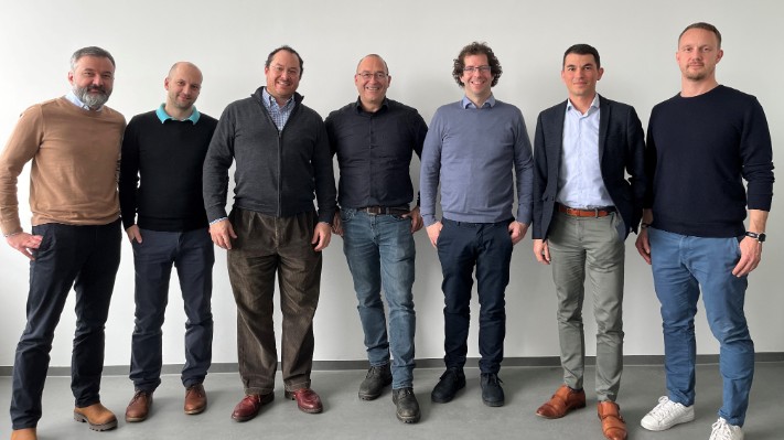
To jointly provide in-situ characterization tools, solutions and services, the companies Alemnis, Imina Technologies, NenoVision and point electronic have formed an alliance. It is further strengthened by principal investigator specialized on in-situ techniques, Prof. Dr. Marc-Georg Willinger.
Electron Microscopy (EM) is widely used across different disciplines in research and engineering. Since its early days, EM has advanced amazingly. Nowadays, the users are not limited by imaging and related analysis but can add more techniques, such as AFM, electrical probing, sample manipulation and force sensing. As providers of leading tools used in-situ in combination with electron microscopy, we decided to form an alliance, bringing our technology under one umbrella.
Why the In-situ Microscopy Alliance?
The In-situ Microscopy Alliance (IMA) was founded to share know-how and technology for in-situ microscopy and testing, to accelerate innovation and adoption of new techniques and to foster new applications across disciplines.
Our mission is to connect industry and academia to advance the in-situ microscopy characterization tools, solutions, and services.
As an alliance, we will:
- Create an ecosystem to enable leading industrial and academic players to explore, develop and promote in-situ characterization techniques, tools, and applications.
- Educate the research and engineering community about the capabilities of in-situ characterization techniques.
- Offer integrations of advanced analytical tools and applications for comprehensive in-situ characterization.


A Word from Our Advisor
We are very proud to have a leading in-situ microscopy researcher on board. Together, we aim to develop the alliance and address the most relevant needs of microscopy users.
Why did you join the In-situ Microscopy Alliance?
Capturing the whole picture and different aspects from the nm to mm scale is a challenging and complex task.
New technology and miniaturization of various techniques in the last years enabled us to reach the technology level to make real in-situ SEM microscopy accessible. Now is the time to harvest this opportunity, and I can't resist being a part of it.
Why do you think that in-situ analysis will enable progress in particular fields?
To study functional materials in their applicable state is crucial to understand their natural function, especially if we talk about game-changing technologies for batteries, catalysis, and corrosion processes.

Alemnis AG
Alemnis develops instruments for mechanical testing at the micro- and nanoscale. The Alemnis Standard Assembly (ASA) works with true displacement control in addition to standard load control mode. With a range of ultra high strain rate modules, users can test at strain rates of up to 20'000/s and millions of impact test cycles.
Products are compact and ideally suited for in-situ experiments as well as ex-situ as a standalone setup. The ASA can be installed in various kinds of microscopes such as Scanning Electron Microscopes (in-SEM), Light Microscopes (in-Air), in Synchrotron, Raman, X-ray tomography, and in nuclearized hot labs, as well as combined with the Nenovision LiteScope™ (for combined in situ AFM with nanoindentation).

Nenovision
NenoVision develops and fabricates LiteScope™, a unique AFM for integration into SEMs. LiteScope enables multimodal & correlative in-situ sample analysis at the nanoscale.
It allows precise localization of the region of interest to measure the mechanical, electrical and magnetic properties of samples inside your SEM. The combination of AFM and SEM represents an ideal solution in the field of Battery research, 2D materials, Semiconductors, Steel & Alloys, Powders & Particles, Life Science, etc.

