SEM Electrical Analysis
Electrical Analysis system for high-quality visualization of electronic properties and defects
EA for SEM system is used for research and development of a wide range of novel devices, from large-area solar cells, photovoltaics, optoelectronics and high-power transistors to nanometer sized wires, pillars and dots.
The system is a turnkey solution compatible with most SEM and FIB-SEM, packaged with own hardware and software, including dedicated sample holder, amplification, voltage biasing and simultaneous imaging, so that electrical activity is recorded with highest speed and lowest noise.
It is designed for quantitative measurements, therefore electronics are factory calibrated and the software is designed for automated metadata management and measurements.
The system consists of hardware, software and selectable options.
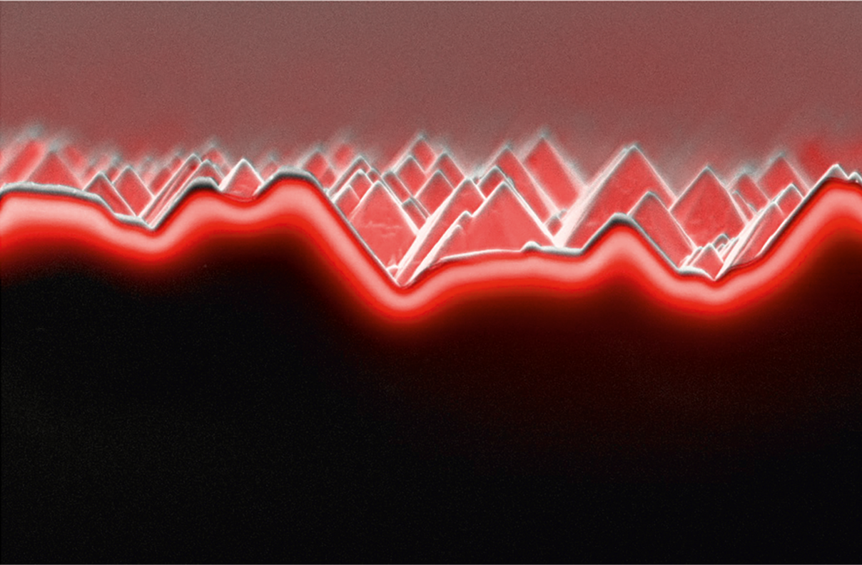
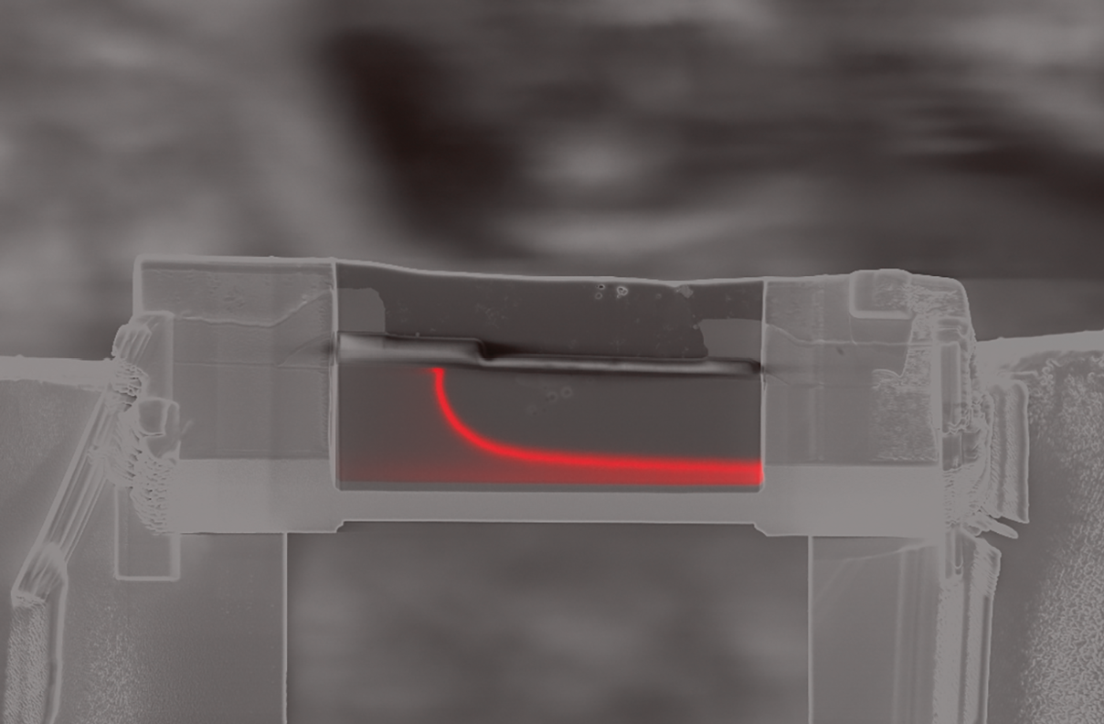
Internal electric fields
- Map active areas of junctions and contacts
- Validate doping profiles against design or model
- View electrical behaviour under bias
- Export data for quantification of diffusion length
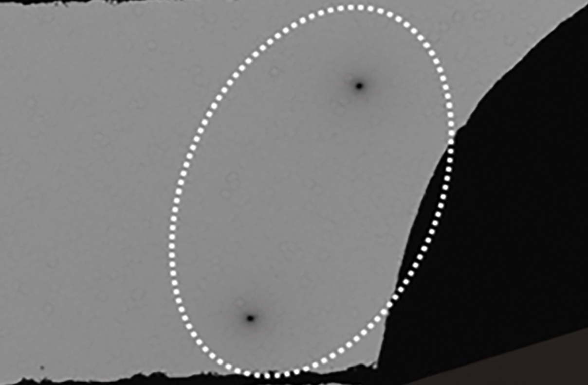
Electrical activity of defects
- Localise sites with increased recombination activity
- Continue with high-resolution microscopy techniques
- Export data for quantification of recombination strenght
Range of techniques
- Electron Beam Induced Current (EBIC)
- Electron Beam Absorbed Current (EBAC)
- Resistive Contrast Imaging (EBAC/RCI)
- Electron Beam Induced Resistance Change (EBIRCh)
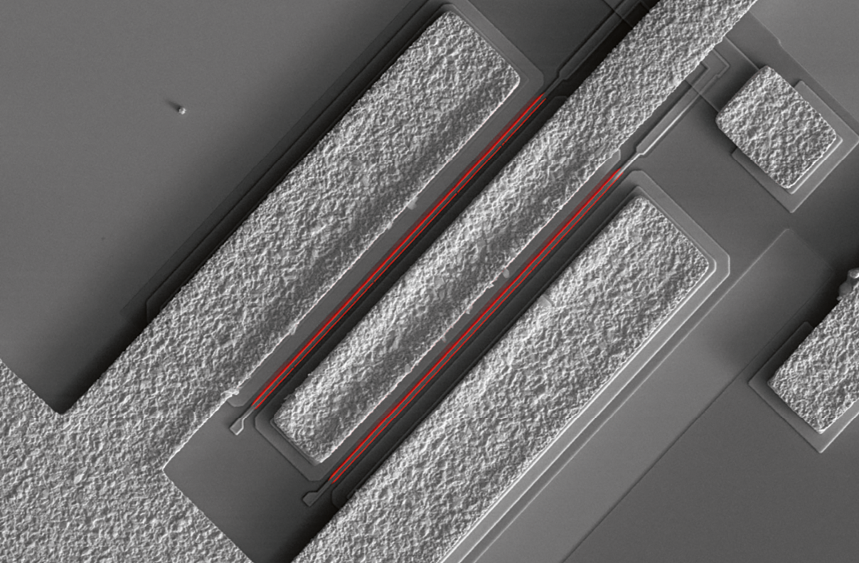
Resistance mapping
- Map spatial distribution of electrical resistance
- Identify shorts and opens in devices
- Localise weaknesses and leakage paths
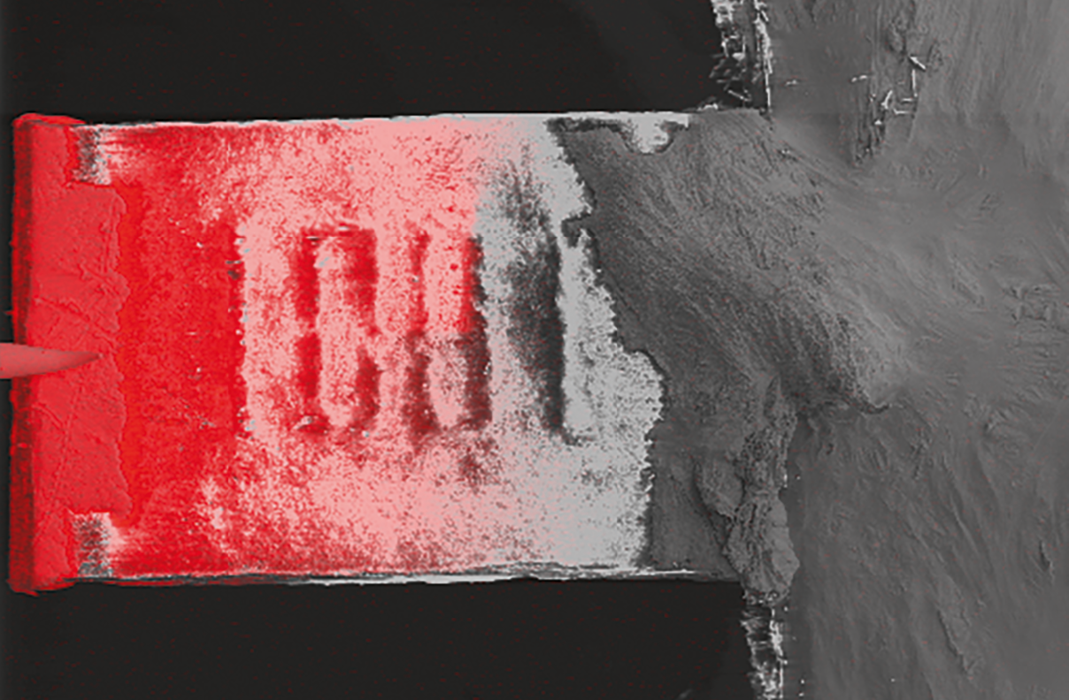
TEM sample screening
- Exploit wide field-of-view in SEM to select target
- Use EA live in FIB/SEM to prevent preparation errors
- Screen lamellas in SEM before transfer to TEM
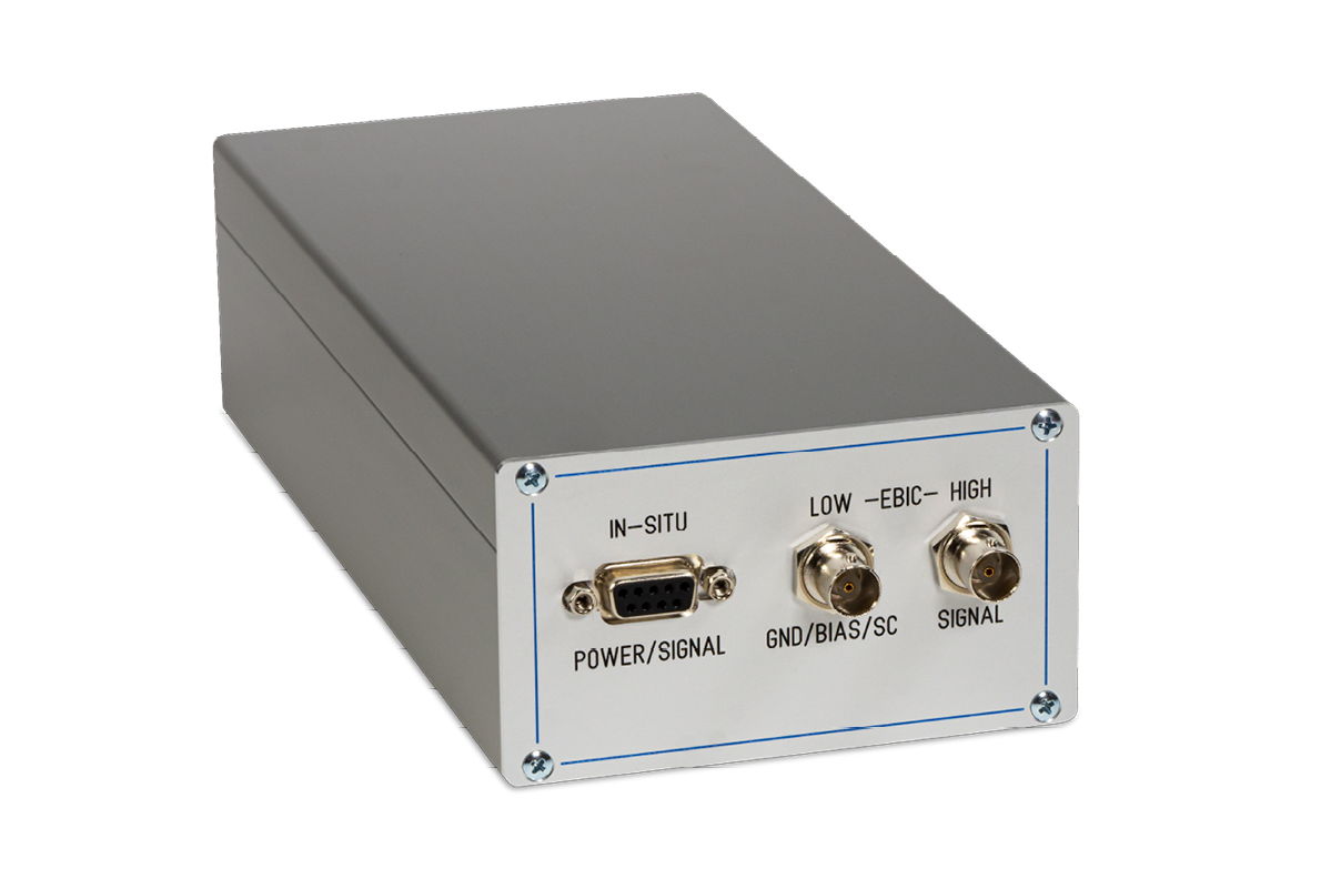
EA Amplifier
- Calibrated high-speed electronics, with in-situ and ex-situ preamplifiers
- Complex multi-stage amplification for imaging, with automatic low-pass filter
- Integrated pico-ammeter for beam current measurements
- Integrated voltage source for biasing
- Integrated current source for compensation
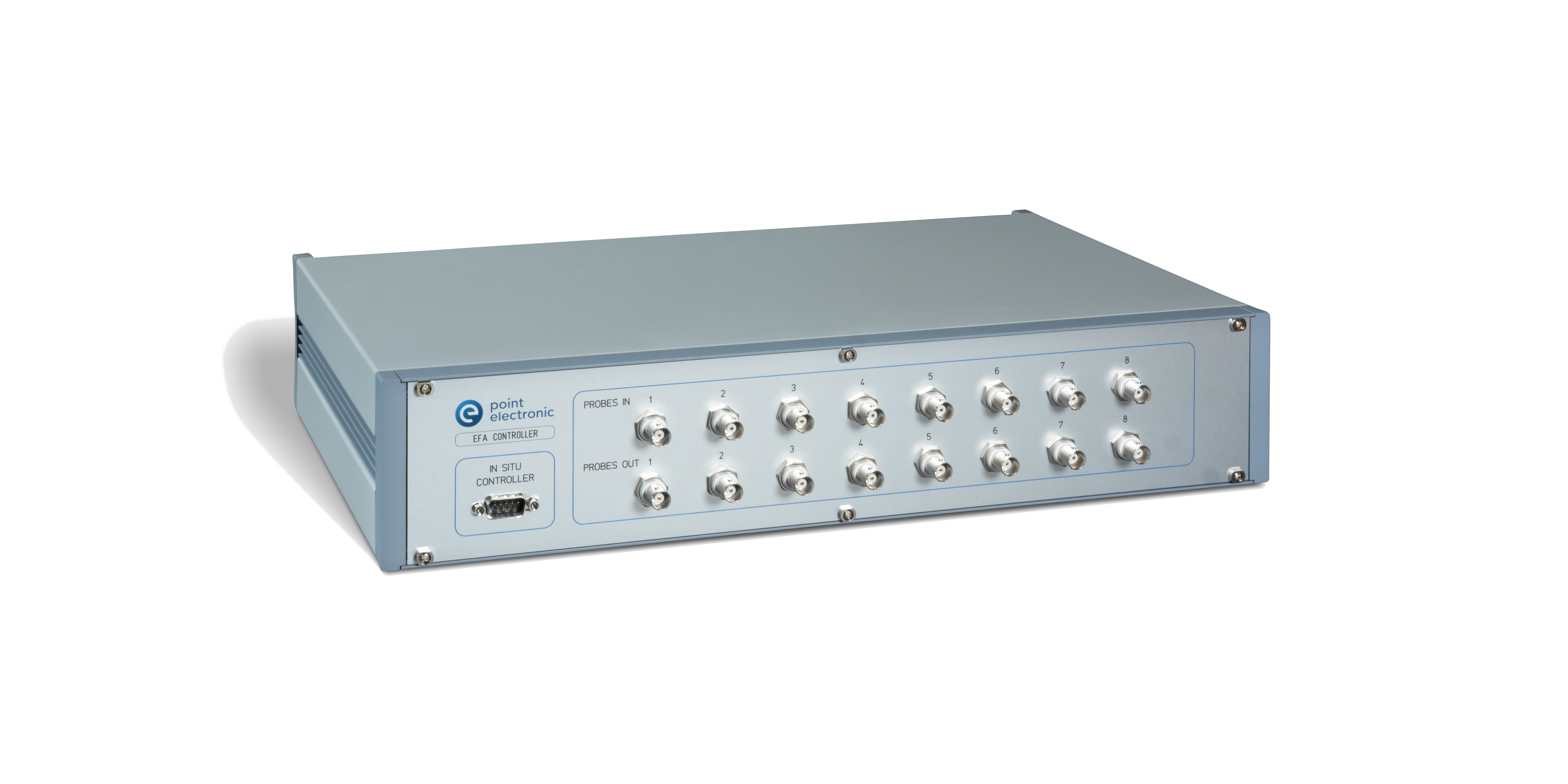
EFA controller
- High-speed multi-stage amplification for imaging, with automated low-pass filter
- Automated signal switch-board for routing
- Automated pico-ammeter for beam current measurements
- Integrated voltage and current sources for biasing and compensation
- Optional low- and high-power PSUs for probe cleaning
- Optional in-situ preamplifiers for low-impedance failure cases
- Optional Current-Voltage (IV) sweeps
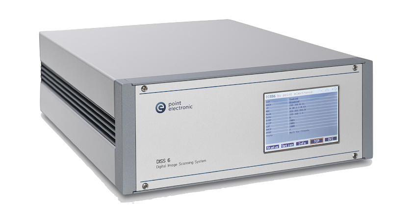
DISS6 SEM Scan Controller
- Latest generation electronics for image scanning
- Calibrated 16-bit signal digitization
- Standard 4x simmultaneous SEM signal inputs
- Added 8x simmultaneous inputs for in-situ preamplifiers
- Independent brightness & contrast controls for each signal
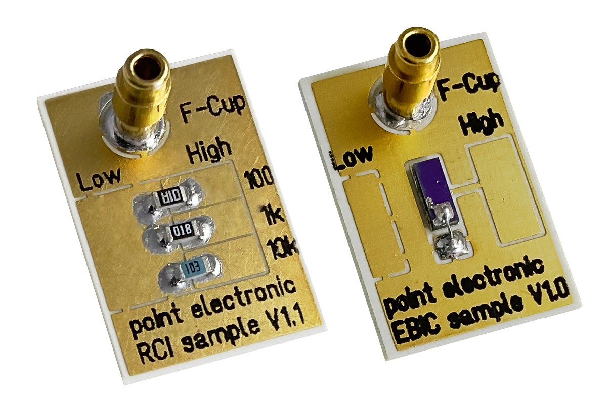
EA/EFA reference samples
- diode and resistors for reference and training
- surface mounted onto ceramic board for easy handling
- integrated Faraday cup for beam current measurements
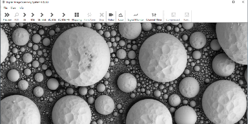
DISS6 image acquisition
- Integrated software for image acquisition and amplifier control
- Advanced tools for colour mixing, current-voltage (IV) and line scans
- Inspection and export functions of calibrated image data
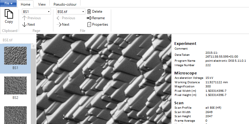
DIPS6 image processing
- Dedicated software for display of image data
- Inspection of acquisition settings in metadata
- Extraction of quantitative pixel value
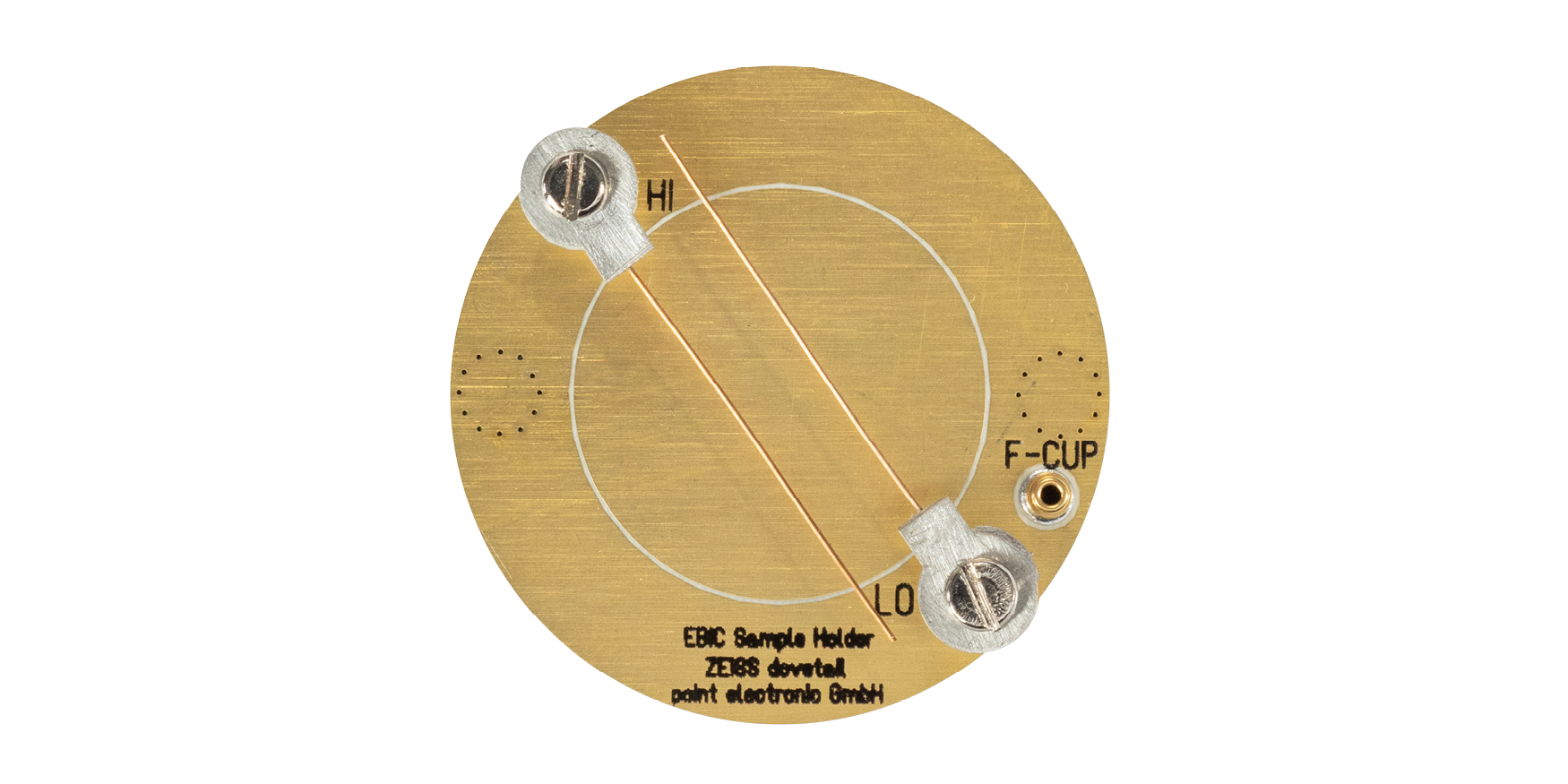
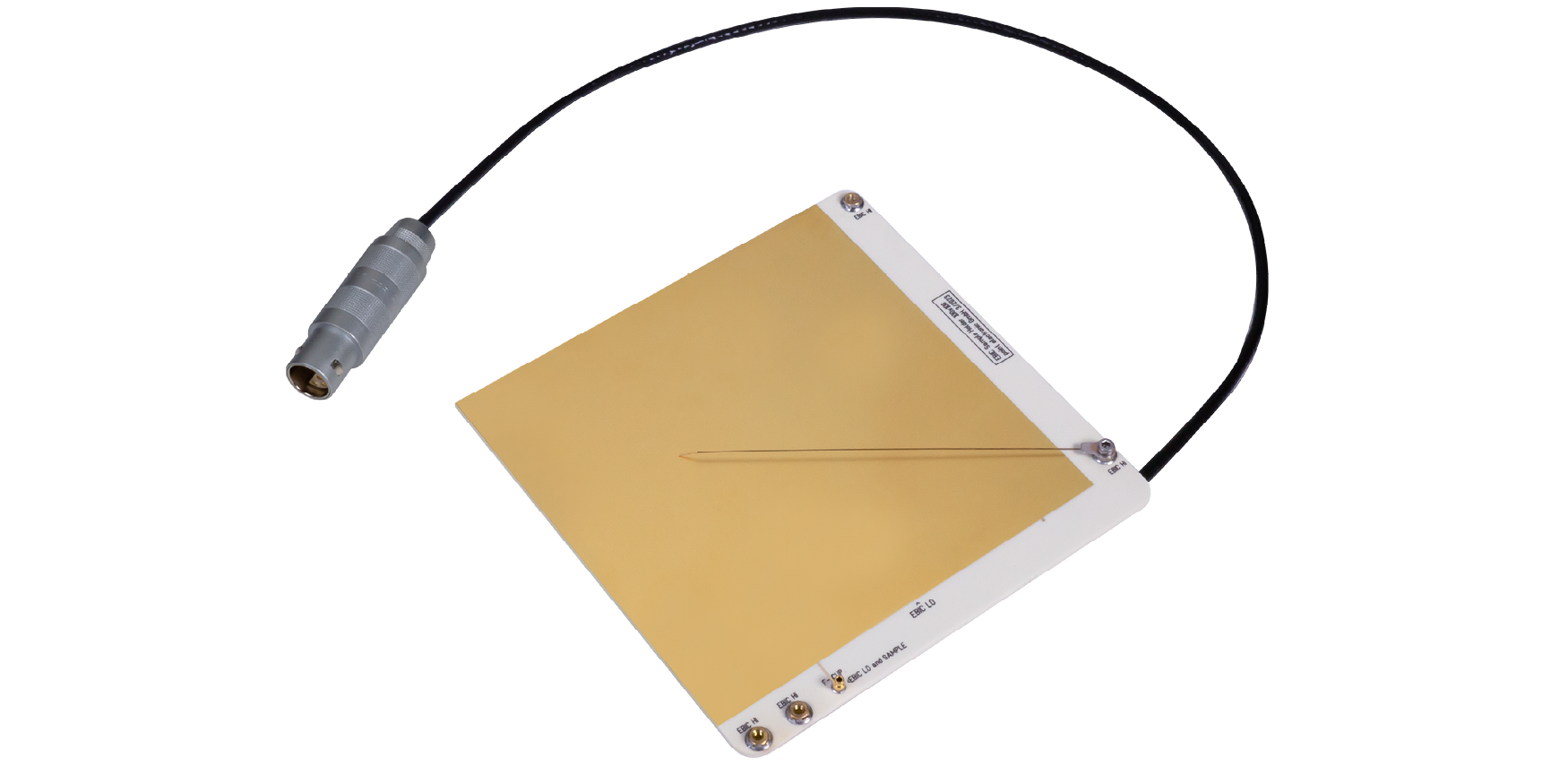
EA sample holders
- 2x probes for ex-situ preamplifier
- Cross-sectional and plan-view mounts
- Integrated Faraday cup
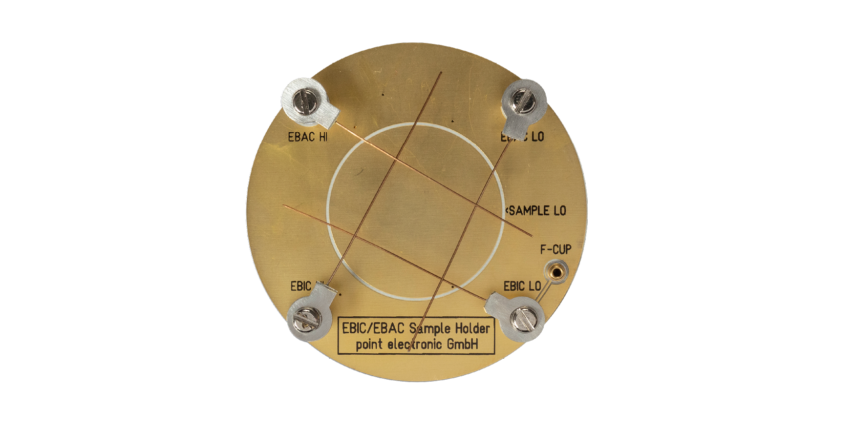
Premium EA sample holder
- 2x probes for ex-situ preamplifier
- 2x probes for ex-situ preamplifier
- Cross-sectional and plan-view mounts
- Integrated Faraday cup
Custom sample holder
- Sample holders for various applications on request.