Automated and Adaptive Manufacturing Processes for TEM Sample Preparation in Microelectronics
Joint project to develop an automated, end-to-end workflow for TEM sample preparation. The Goal: reduce manual intervention, standardize processesm and significantly improve reproducibility.
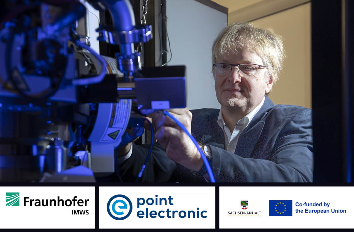
Every day, countless samples are examined for quality control in the world’s largest semiconductor factories. Due to the small size of modern microelectronic components, this is often done using high-resolution transmission electron microscopy (TEM). The production of the samples is very labor-intensive and often still requires a considerable amount of manual process control and expert knowledge. The Fraunhofer Institute for Microstructure of Materials and Systems IMWS in Halle (Saale) and point electronic GmbH now aim to jointly develop novel high-throughput fabrication processes for TEM samples that offer exceptional speed, improved automatability, and high precision.
Cars are packed with electronics, as are smartphones. Household appliances are connected, and artificial intelligence is creating entirely new possibilities in many industries. All these developments rely on powerful and reliable microelectronic components and processors. Fundamental to this is the ability to precisely structure and functionalize materials down to the scale of a few nanometers. Transmission electron microscopy (TEM) is therefore an indispensable tool for quality control and in the development of new products: This method provides insights into the smallest details with the highest spatial resolution.
For TEM examinations, material samples must first be prepared using complex methods. The procedures involved must be extremely precise, require a great deal of practical expertise, and are time-consuming. Given the growing demand for TEM analyses, automated and adaptively controlled sample preparation processes could offer decisive advantages and significantly increase throughput. The “Adaptive Milling” project, which runs through February 2027, aims to develop such a process.
“High sample throughput is crucial, especially in industrial applications - our approaches are specifically tailored to meet this need," says Christoph Sichting, CEO of point electronic GmbH. “The approach we are jointly pursuing combines three innovative concepts into a comprehensive system characterized by high precision, automatability, and efficiency,” adds Dr. Richard Busch, who is leading the project at Fraunhofer IMWS.
The results will include hardware, software algorithms, and databases. point electronic GmbH is contributing its expertise in the development and manufacture of analysis systems and functional extensions for electron microscopy. The expertise available at Fraunhofer IMWS in the application of electron microscopy methods as well as the development of sample preparation workflows and equipment are also key components for the project’s success.
“In addition to solutions for individual components, we also need to develop highly complex process logic. But the challenge is well worth it! With our innovative preparation system, we are providing a highly capable tool that, given the very high number of TEM analyses conducted worldwide, can make a significant contribution to improving material analysis in the field of microelectronic components as a whole. Our approach has the potential to take high-throughput preparation of TEM sections to a new level,” says Busch.
“Semiconductors are no longer a niche technology - with this project, we are helping to manage the rapidly growing demand for analysis," says Sichting. “Thanks to our compatibility approach, our systems can be installed on a wide range of devices regardless of the manufacturer - this flexibility enables us to achieve deep market penetration and widespread adoption of the technology in the future.”