Publication about the first combined use of 4D-STEM and STEM-EBIC techniques
"In-Operando 4D-STEM and STEM-EBIC Imaging of Electric Fields and Charge Carrier Behavior in Biased Silicon p–n Junctions.", published in Advanced Electronic Materials.
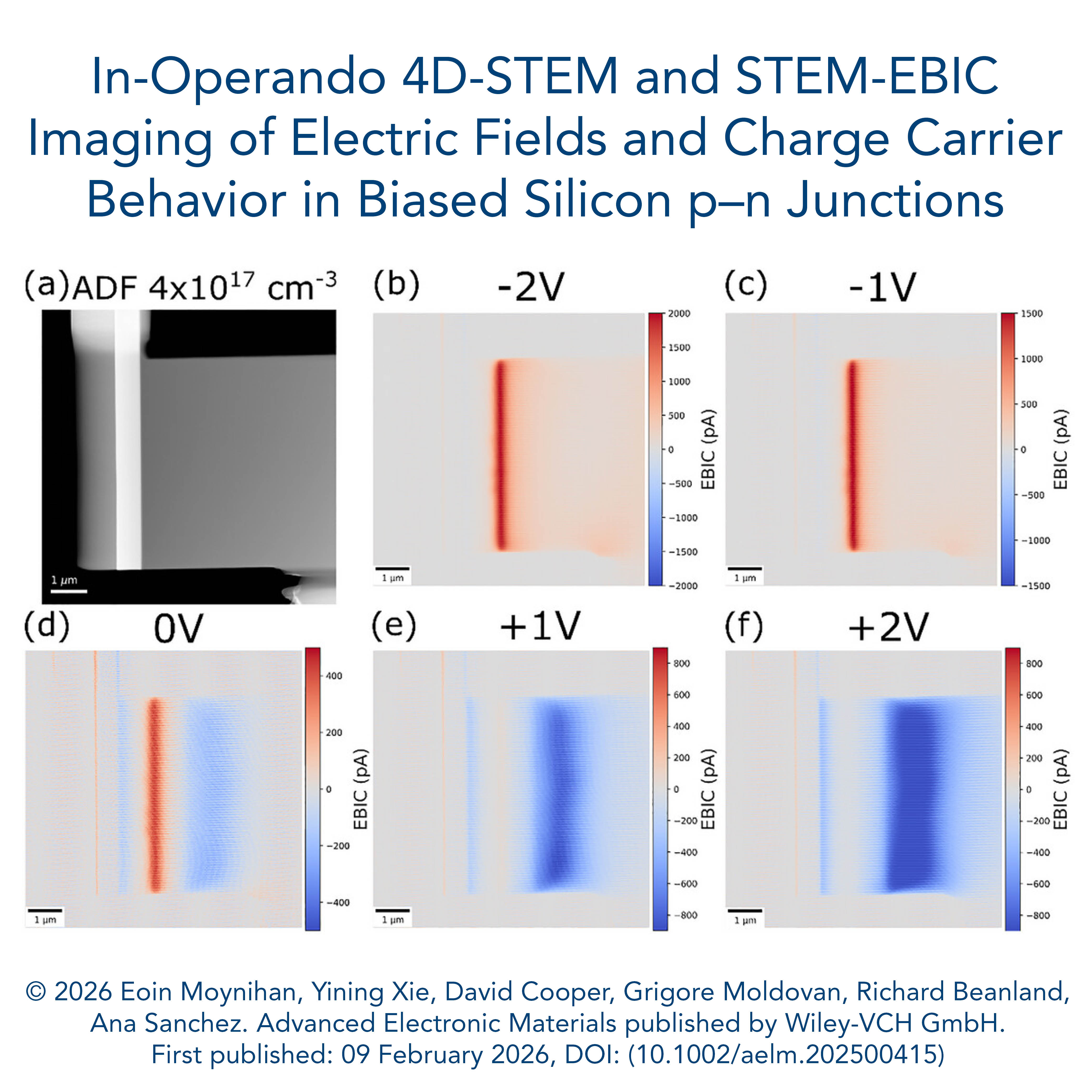
An inspiring new article on in-operando TEM by the Microscopy Group of the University of Warwick reveals the first combined use of 4D-STEM and STEM-EBIC techniques.
Dr. Eoin Moynihan, Prof. Ana M Sanchez, Richard Beanland, and their team used quantitative analysis supported by simulations to show that the two techniques in correlation enable robust interpretation of electric field strength, field direction, built-in potential, and minority carrier diffusion length - directly in the TEM.
The new study addresses long-standing challenges and lays a key foundation for the future of nanoscale electrical analysis of devices in TEM.
We at point electronic GmbH are proud that our Electrical Analysis system for TEM played a key role in this fantastic study. Quantitative measurements and open data are key aspects of our electronics and software, not only for TEM, but also for SEM, and they prove again as a key enabler for in-operando work.
Congratulations to Eoin Moynihan, Ana Sanchez, and the entire University of Warwick microscopy team, as well as David Cooper from CEA-LETI Université Grenoble Alpes, and Yining Xie for this leading contribution.
Find the full paper published at Advanced Electronic Materials:
arcticle In-Operando 4D-STEM and STEM-EBIC
(Adv Elect Materials, First published: 09 February 2026, DOI: (10.1002/aelm.202500415)