Workshop: SEM Nanoprobing and Electrical Failure Analysis for Semiconductors
May 18, 2026
- Fraunhofer IMWS
- Halle (Saale), Germany
- cam-workshop.de
About the Workshop
Device characterization and failure analysis workflows for advanced semiconductor technology.
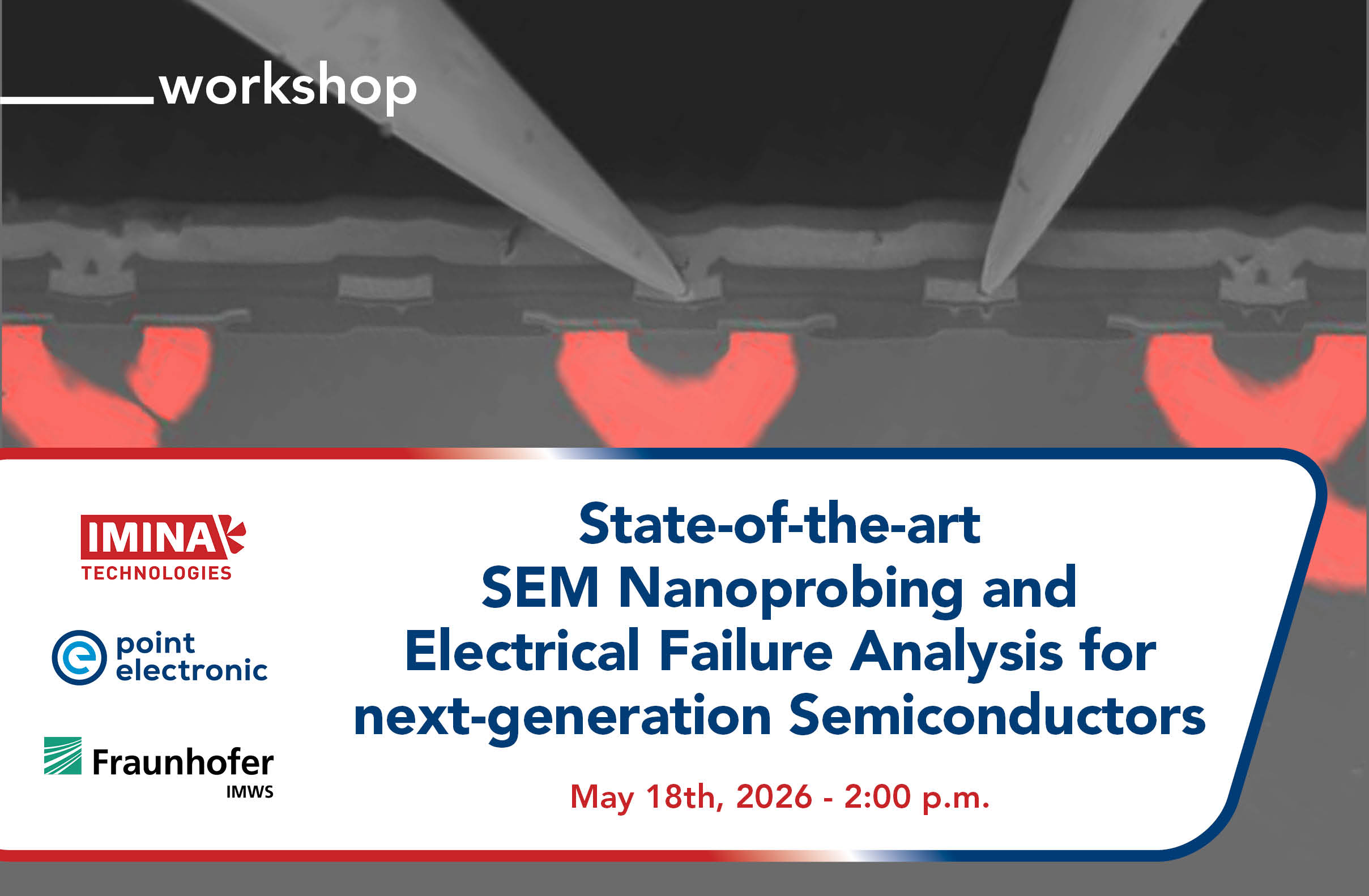
This joint Imina Technologies and point electronic workshop, held in cooperation with Fraunhofer IMWS, demonstrates our latest in-situ SEM nanoprobing and electrical failure analysis (EFA) hard- and software. Our fully integrated Nanoprobing and EFA solution offers streamlined workflow designed to shorten the learning curve, simplify sample characterization, and save time.
We will present fast and precise sample navigation and characterization, low-noise signal acquisition, and multi-channel failure detection with in-situ pre-amplifiers and live color-coded signal overlay. Our application experts and system users from Fraunhofer IMWS will share insights about their experiences with different applications.
Some specific measurements you can expect in the demo:
- Quickly navigating the sample and precisely landing the probes to establish stable electrical contact;
- Measurements of IV, leakage, etc, with guided step-by-step workflows;
- Advanced EFA with low-noise Resistive Contrast Imaging (RCI) and other electron beam collecting techniques.
Presented by:
Event Pricing
The workshop is free of charge, and will also include a guided tour around Fraunhofer IMWS.
It can be attended without participating in the CAM workshop.
To attend, your registration is required.
Event Time and Location
Monday, May 18th, 2026
2 p.m. – 5:30pm
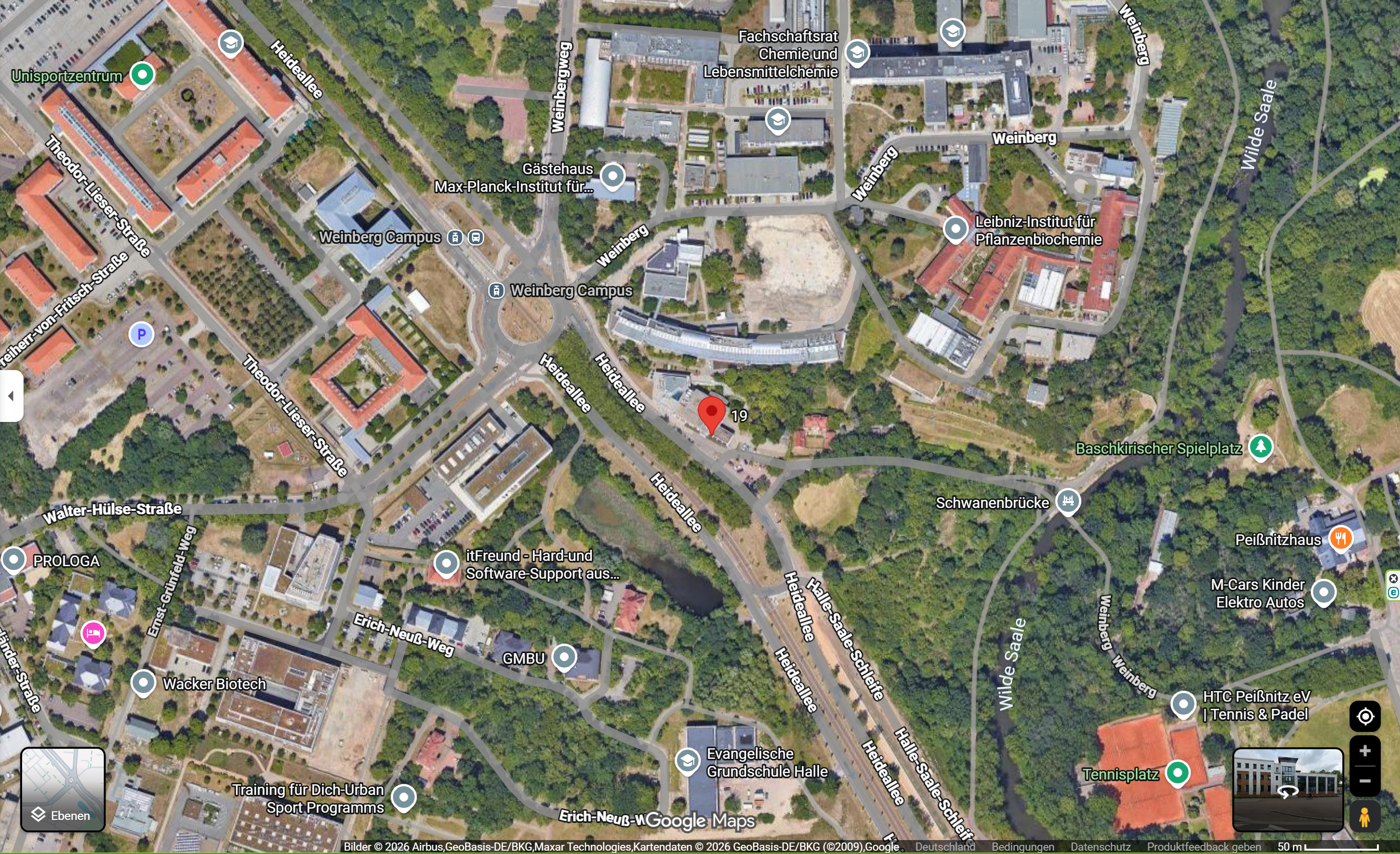
Fraunhofer IMWS building, Heideallee 19, 06120 Halle (Saale)